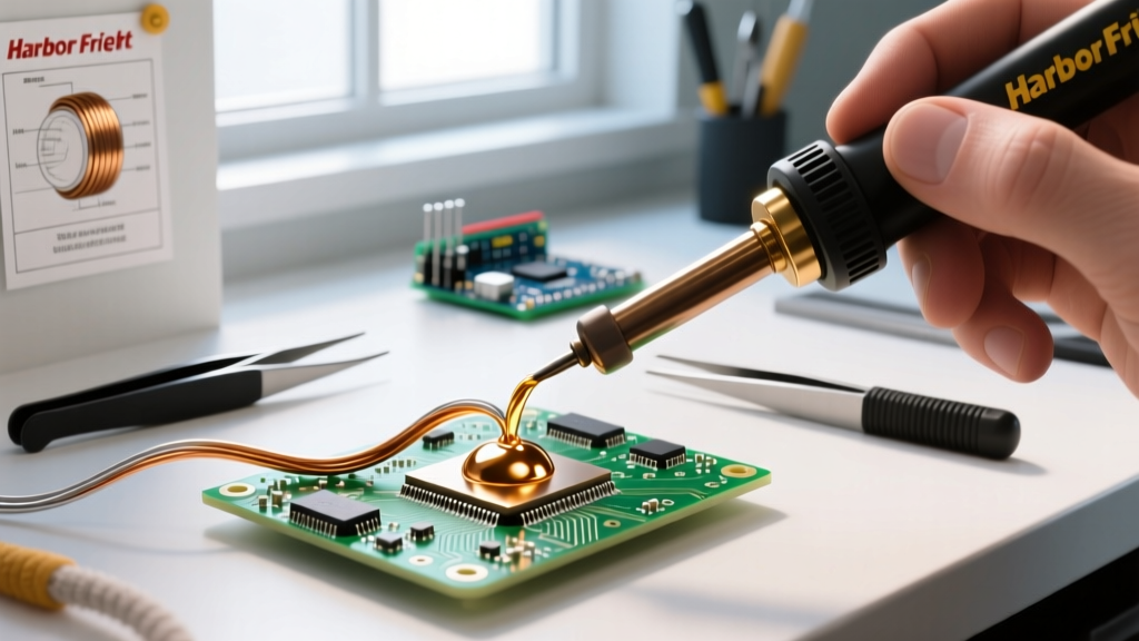

Removing a component from a printed circuit board (PCB) is inherently more destructive and complex than soldering one on. While soldering relies on capillary action and wetting, desoldering requires breaking those metallurgical bonds without destroying the fragile copper pads or the FR-4 fiberglass substrate. Whether you are salvaging vintage audio gear or reworking a dense BGA layout, mastering this reverse process is non-negotiable for any electronics technician.
The Metallurgy of Solder Removal
Before touching an iron to a board, you must understand the enemy: oxidation and intermetallic compounds (IMCs). Over time, and especially after multiple thermal cycles, the tin in your solder reacts with the copper pad to form a brittle Cu6Sn5 layer. When attempting desoldering on older boards or lead-free assemblies, this IMC layer raises the effective melting point and prevents the solder from flowing smoothly into your extraction tool.
This is why the first rule of professional desoldering is counterintuitive: add fresh solder before removing the old. By introducing fresh, flux-cored 63/37 tin-lead solder, you dilute the lead-free or oxidized alloy, lowering its melting point and restoring fluid dynamics. According to the IPC-7711/7721 standards for rework and repair, managing the thermal profile and chemical flux activity is the primary determinant of a successful, pad-safe removal.
Desoldering Arsenal: Tool Selection Matrix
Choosing the wrong tool is the fastest route to a lifted pad. Below is a breakdown of the primary extraction methods, their ideal use cases, and the specific models trusted by bench professionals.
| Tool Type | Best Application | Recommended Model | Typical Cost | Risk Factor |
|---|---|---|---|---|
| Desoldering Pump (Sucker) | Through-hole DIPs, large electrolytic capacitors | Engineer SS-02 | $18 - $25 | Medium (Mechanical shock) |
| Copper Desoldering Braid | Final pad cleanup, small SMD passives | Chemtronics 80-1-5 (No-Clean) | $8 - $12 | High (Pad tearing if dragged) |
| Hot Air Rework Station | Multi-pin SMD ICs, QFP, SOIC | Quick 861DW | $220 - $260 | High (Thermal damage to nearby parts) |
| Desoldering Tweezers | 0402 to 0805 SMD resistors/capacitors | Hakko FX-303 (with tweezers) | $150 - $180 | Low |
Phase 1: Through-Hole Desoldering Protocol
Through-hole components possess high thermal mass, especially on multi-layer boards with internal ground planes. A standard 40W iron will fail here. You need a temperature-controlled station capable of rapid thermal recovery.
Step 1: Chemical Preparation
Apply a high-quality tacky flux, such as Amtech NC-559-V2, directly to the joints. Do not rely on the flux inside your solder wire; you need a generous external reservoir to break down existing oxides and promote capillary wicking.
Step 2: The Alloy Dilution Trick
Feed a small amount of fresh 63/37 Leaded solder onto the existing joint. If the board is RoHS-compliant (lead-free), the original solder likely melts around 217°C to 227°C and oxidizes rapidly. The fresh leaded solder drops the eutectic melting point to 183°C, making the joint highly fluid.
Step 3: Heat and Extract
Set your iron (e.g., Hakko FX-951 with a C4 tip) to 360°C. Apply the tip to the pad, ensuring maximum surface contact. Wait exactly 2 to 3 seconds for the solder to liquefy completely. Immediately press the nozzle of your Engineer SS-02 desoldering pump firmly against the molten pool and trigger the release. The mechanical vacuum will pull the liquid solder into the PTFE-lined cylinder.
Step 4: Component Liberation
Once all pins are cleared, gently push the component from the opposite side. If a pin resists, do not force it. Forcing a cold pin will rip the copper barrel out of the plated through-hole (PTH). Reapply flux, reheat, and use a wooden toothpick to gently clear any residual solder from the hole.
Phase 2: Surface Mount (SMD) Extraction
SMD desoldering relies on uniform heat distribution rather than mechanical vacuum. Using a soldering iron on a 64-pin QFP chip will result in broken traces and frustration.
Masking and Fluxing
Surround the target IC with Kapton (polyimide) tape to protect adjacent components from convective heat. Flood the pins with liquid or gel flux. The flux acts as a thermal bridge, ensuring heat transfers evenly across all pins simultaneously.
Hot Air Parameters
For a standard Quick 861DW station, set the temperature to 350°C with an airflow rate of 50 (approx. 40 liters/minute). Use a nozzle that is slightly larger than the IC body. Hold the wand exactly 10mm above the chip, moving in small, continuous circles. Never hold the wand stationary, as localized hot spots will delaminate the PCB substrate.
The Lift-Off
After 15 to 30 seconds of circular heating, gently nudge the IC with fine-point titanium tweezers. If the chip moves freely on its surface tension, it is ready. Lift it straight up. If it snags, the center thermal pad (common on QFN packages) is not yet molten. Continue heating for another 5 seconds and test again.
Expert Warning on QFN Packages: Quad Flat No-lead (QFN) packages feature a hidden ground pad underneath the chip. This pad requires significantly more thermal energy to melt than the perimeter pins. Pre-heating the bottom of the PCB with a specialized mat (like the Hakko FR-810B) at 150°C drastically reduces the top-side hot air time required, saving sensitive silicon from thermal death.
Catastrophic Failure Modes and Avoidance
Even with the right tools, desoldering carries inherent risks. Understanding these failure modes allows you to intervene before permanent damage occurs, a frequent topic in EEVblog's extensive bench rework tutorials.
Lifted Pads and Trace Delamination
The epoxy resin binding the copper foil to the FR-4 core loses its adhesive strength at temperatures exceeding 260°C. If you dwell with a 400°C iron for more than 5 seconds, the pad will lift. Prevention: Use the largest iron tip possible to maximize thermal transfer speed, minimizing dwell time.
Plated Through-Hole (PTH) Barrel Tearing
When using copper braid to clean a through-hole, technicians often drag the braid across the hole with downward pressure. This acts like a razor blade, slicing the copper barrel. Prevention: Always use a fresh, flux-saturated piece of braid. Let the capillary action do the work; the iron's weight should be the only downward pressure applied.
Thermal Shock to Silicon
Semiconductor junctions degrade rapidly past 150°C internally. While the solder melts at 183°C+, the internal die can reach critical failure thresholds if heated for prolonged periods. Prevention: Utilize board pre-heaters to bring the ambient baseline of the PCB to 100°C. This means your localized hot air or iron only needs to add a delta of 80°C to 100°C to achieve reflow, rather than a brutal 200°C delta from room temperature.
Final Board Cleanup and Inspection
Once the component is removed, the board is rarely ready for immediate rework. Residual flux and microscopic solder spheres remain.
- Braid Wash: Use a 2mm Chemtronics no-clean braid to gently wick away the final microscopic layer of solder from the pads. Ensure the pads remain flat; any bumps will prevent the new component from seating correctly.
- Solvent Scrub: Apply 99% Isopropyl Alcohol (IPA) and scrub vigorously with a stiff ESD-safe brush. This removes activated flux residues that could cause electrochemical migration (dendrite growth) over time.
- Optical Inspection: Under a 10x to 40x stereo microscope, inspect the PTH barrels for internal tears and verify that no adjacent SMD passives were accidentally shifted or tombstoned during the hot air process.
Mastering desoldering transforms you from a simple assembler into a true PCB rework technician. By respecting the metallurgy, controlling your thermal profiles, and utilizing the correct extraction mechanics, you can salvage and repair boards that others would discard as scrap. For further reading on foundational techniques, refer to SparkFun's electronics lab guides.