
Beyond the Melt: The True Metallurgy of Soldering
When most beginners ask, "how does soldering work?", they are usually looking for a simple mechanical explanation: heat the metal, melt the wire, and let it cool. However, from an electrical engineering and materials science perspective, soldering is not merely a mechanical glue. It is a complex metallurgical bonding process that relies on atomic diffusion, chemical reduction, and precise thermal dynamics.
Unlike welding, which melts the base metals to fuse them, soldering operates below the melting point of the substrate. As of 2026, the electronics industry relies heavily on lead-free alloys and advanced no-clean fluxes governed by strict IPC J-STD-001 requirements. To master soldering—whether you are using a $60 Pinecil or a $400 Hakko FX-951 station—you must understand the invisible physics and chemistry occurring at the solder joint interface.
The Physics of Wetting and Capillary Action
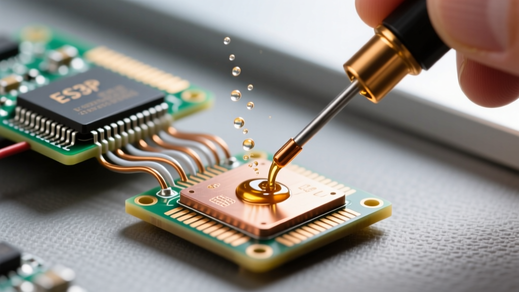
The foundational principle of how soldering works is wetting. Wetting is the ability of a liquid to maintain contact with a solid surface, resulting from intermolecular interactions. In soldering, liquid solder must displace surface contaminants and spread across the copper pad or component lead.
Understanding the Contact Angle
Wetting is measured by the contact angle (θ) where the liquid solder meets the solid substrate:
- θ < 30°: Excellent wetting. The solder flows out smoothly, creating a strong, concave fillet (ideal for IPC Class 3 high-reliability assemblies).
- 30° < θ < 90°: Acceptable wetting. The joint is mechanically sound but lacks optimal capillary penetration.
- θ > 90°: Poor wetting (non-wetting). The solder beads up like water on a waxed car, resulting in a mechanically weak and electrically resistive joint.
In Plated Through-Hole (PTH) components, wetting drives capillary action. The liquid solder is drawn upward into the barrel of the hole. For a compliant IPC Class 2 joint, solder must wet at least 75% of the barrel height; for Class 3 (aerospace/medical), it requires 100% barrel fill.
The Chemical Catalyst: How Flux Actually Works
Solder will not wet oxidized copper. The moment bare copper is exposed to air, it forms a layer of copper oxide (CuO and Cu2O), which acts as a barrier to atomic bonding. This is where flux becomes the most critical variable in the soldering process.
Expert Insight: Flux is not a cleaning agent for dirt or oils; it is a chemical reducing agent designed specifically to strip metallic oxides at elevated temperatures and prevent re-oxidation while the solder is molten.
Flux Chemistries in Modern Electronics
According to data from major manufacturers like Kester and Alpha Assembly, modern fluxes fall into three primary categories:
- Rosin (R) and Rosin Mildly Activated (RMA): Derived from pine tree sap (abietic acid). When heated above 120°C, abietic acid becomes mildly acidic, dissolving copper oxides. It becomes inert upon cooling, making it safe to leave on the board.
- No-Clean (NC): The dominant standard in 2026. These use synthetic resins and weak organic acids. They are engineered to volatilize or encapsulate upon cooling, leaving a clear, non-conductive, non-corrosive residue that does not interfere with in-circuit testing (ICT).
- Water-Soluble (OA - Organic Acid): Highly active fluxes used for heavily oxidized parts or wave soldering. They must be cleaned with deionized water post-soldering, as the residue is highly conductive and corrosive.
The Intermetallic Compound (IMC) Layer
If you want to know how soldering works at an atomic level, you must understand the Intermetallic Compound (IMC) layer. Soldering does not just "stick" metals together; it creates a new, distinct metallurgical phase at the boundary.
When molten tin (Sn) contacts solid copper (Cu), the tin atoms dissolve the copper surface. As they cool, they form two distinct intermetallic layers:
- Cu6Sn5 (Eta phase): Forms immediately at the solder-copper interface during the molten state. It is relatively ductile and essential for a strong bond.
- Cu3Sn (Epsilon phase): Forms between the copper and the Cu6Sn5 layer, primarily during thermal aging or prolonged heating.
The Danger of IMC Overgrowth
An IMC layer is necessary, but it is inherently brittle. An ideal IMC layer is between 1 to 3 micrometers (μm) thick. If a technician applies too much heat, or holds the iron on the pad for too long, the IMC layer grows excessively thick. This results in a brittle joint prone to mechanical fracturing under thermal cycling or physical shock—a common failure mode in poorly executed hand-soldering.
Alloy Profiles: Thermal Dynamics and Melting Points
The choice of solder alloy dictates your thermal profile. Applying the wrong temperature will either fail to initiate wetting or destroy the PCB's FR4 substrate and component internals.
| Alloy Designation | Composition | Melting Point | Optimal Iron Temp | Primary Use Case (2026) |
|---|---|---|---|---|
| SAC305 | 96.5% Sn, 3.0% Ag, 0.5% Cu | 217°C - 220°C | 320°C - 350°C | Standard commercial lead-free SMT and hand soldering. |
| Sn60Pb40 | 60% Sn, 40% Pb | 183°C - 190°C | 270°C - 300°C | Hobbyist, prototyping, and exempt military/aerospace. |
| Sn63Pb37 | 63% Sn, 37% Pb (Eutectic) | 183°C (Single phase) | 270°C - 300°C | Precision hand soldering; prevents plastic-range disturbance. |
| Sn42Bi58 | 42% Sn, 58% Bismuth | 138°C | 200°C - 220°C | Low-temp soldering, heat-sensitive components, LED strips. |
Note: The optimal iron temperature is always significantly higher than the alloy's melting point. This "superheat" is required to overcome the thermal mass of the PCB ground planes and component leads, ensuring the flux activates and the IMC layer forms within a 2 to 4-second dwell time.
Diagnosing Soldering Failure Modes
Understanding the science allows you to diagnose visual defects accurately. The NASA Electronic Parts and Packaging (NEPP) program and IPC standards categorize failures based on their metallurgical root causes:
- Non-Wetting: The solder contacts the surface but draws back, leaving a high contact angle. Root Cause: Heavy oxidation, insufficient flux activation, or inadequate pre-heating.
- Dewetting: The solder initially wets the surface but then retracts into islands or beads as it cools. Root Cause: Contamination (silicones, oils) or a degraded surface finish (e.g., oxidized HASL).
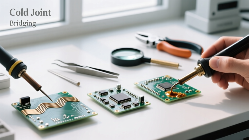
- Cold Joint: A dull, grainy, convex fillet. Root Cause: The joint was disturbed during the plastic (mushy) phase of solidification, or insufficient heat was applied to form a proper IMC layer.
- Tombstoning (SMT only): A surface mount component stands on one end. Root Cause: Uneven wetting forces caused by asymmetric pad heating or uneven paste deposition, pulling the component upright as the solder contracts.
Optimizing Heat Transfer for Perfect Joints
Knowing how soldering works theoretically is only half the battle; executing it requires managing thermal transfer. Modern soldering stations use closed-loop thermocouple feedback in the tip.
When you touch a cold copper pad with a 350°C tip, the tip temperature drops instantly. A high-quality station like the Weller WE1010NA (70W) or JBC CD-2BQE (130W) will detect this drop and inject maximum current into the heating element to recover the temperature within milliseconds.
Pro-Tips for Thermal Management:
- Maximize Surface Area: Always use the largest tip that fits the pad. A chisel tip transfers heat vastly more efficiently than a conical tip due to increased surface contact area.
- Use Solder as a Thermal Bridge: When heating a joint, feed a tiny amount of solder to the intersection of the tip and the pad. The molten solder eliminates microscopic air gaps, increasing thermal conductivity by orders of magnitude.
- Respect the Dwell Time: Aim for 1.5 to 3 seconds per joint. Exceeding 5 seconds risks delaminating the PCB pad, burning the flux, and growing a brittle IMC layer.
Frequently Asked Questions
Why does my solder ball up and refuse to stick?
This is a classic "non-wetting" scenario. The copper surface is oxidized, and your flux has either burned off or is too weak to clean it. Apply fresh flux (like Amtech or Chip Quik tacky flux), lower your iron temperature slightly to prevent burning the new flux, and clean your tip with a brass wire sponge.
Is lead-free solder harder to use than leaded?
Yes. SAC305 has a higher melting point (217°C vs 183°C), a narrower plastic range, and does not flow as easily due to higher surface tension. It requires irons with faster thermal recovery rates and specifically formulated lead-free flux cores to achieve proper wetting.
Can I use plumbing solder for electronics?
Absolutely not. Plumbing solder uses highly acidic, corrosive fluxes (like zinc chloride) designed to clean thick copper pipes. If used on a PCB, the flux residue will rapidly corrode the delicate copper traces and cause short circuits. Always use electronic-grade rosin or no-clean flux core solder.