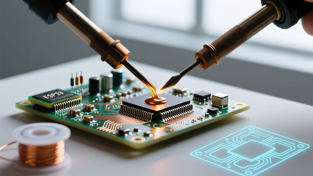

The SMD Assembly Dilemma: Choosing Your Attack Vector
Surface-mount technology (SMT) has largely replaced through-hole components in modern electronics, but assembling fine-pitch integrated circuits (ICs) by hand remains a significant hurdle for prototypers and low-volume manufacturers. Among the various manual and semi-automated techniques, drag soldering stands out as a highly efficient method for specific component geometries. However, it is not a universal panacea. Applying drag soldering to the wrong footprint or production volume will result in catastrophic bridging, lifted pads, and wasted time.
This decision framework is designed to help electrical engineers, DIY enthusiasts, and low-volume assemblers determine exactly when drag soldering is the optimal choice, and when to pivot to solder paste reflow or targeted hot air. By analyzing component pitch, production volume, and thermal requirements, you can select the most reliable and cost-effective assembly method for your 2026 PCB projects.
The Core SMD Assembly Decision Matrix
Before picking up an iron, evaluate your project against the following matrix. This table contrasts drag soldering with the two most common alternatives: solder paste with hot air/reflow, and precision point-to-point micro-soldering.
| Assembly Method | Setup & Tooling Cost | Ideal Component Pitch | Optimal Volume | Primary Limitation |
|---|---|---|---|---|
| Drag Soldering | $110 - $650 (Station + Tips) | 0.50mm to 0.80mm | 1 to 15 boards | Cannot solder hidden bottom pads (QFN/BGA) |
| Solder Paste + Reflow | $400 - $2,500+ (Stencil, Oven) | 0.40mm and below, BGAs | 15 to 1,000+ boards | High upfront cost; stencil management |
| Hot Air + Paste | $150 - $400 (Gun + Paste) | 0.65mm and above, QFNs | 1 to 5 boards | Risk of blowing away adjacent 0402 passives |
| Micro Point-to-Point | $100 - $300 (Fine tip iron) | 0.80mm and above (SOIC) | 1 to 3 boards | Prohibitively slow for 64+ pin ICs |
Scenario A: When Drag Soldering is the Optimal Choice
Drag soldering excels in a very specific intersection of component geometry and production volume. The technique relies on the surface tension of molten solder and the capillary action of high-quality flux to pull solder evenly across a row of pins as a chisel tip glides over them.
Ideal Component Geometries
- Quad Flat Packages (QFP/TQFP): Components like the TQFP-44 (0.8mm pitch) or TQFP-100 (0.5mm pitch) are the quintessential candidates. The gull-wing leads provide an excellent surface for the solder to wet and bridge to the PCB pad.
- Thin Shrink Small Outline Packages (TSSOP): With pitches typically around 0.65mm, TSSOPs drag solder beautifully provided the pads are correctly designed with extended toe and heel fillets.
- SOIC and SOP: While these can be done pin-by-pin, drag soldering a 16-pin SOIC (1.27mm pitch) takes roughly three seconds and eliminates the risk of asymmetric heating.
The Economics of Prototyping
If you are spinning up a batch of five prototype boards featuring an ARM Cortex-M4 microcontroller in a 64-pin LQFP package, ordering a custom laser-cut stainless steel stencil ($150-$250) and setting up a reflow profile is economically unjustifiable. Drag soldering allows you to bypass stencil fabrication entirely, relying only on a high-quality tacky flux, a spool of 63/37 or SAC305 wire solder, and a precision chisel tip. According to SparkFun's SMD Soldering Guide, mastering this technique can reduce per-board manual assembly time by up to 70% compared to pin-by-pin soldering.
Scenario B: When to Reject Drag Soldering
Equally important to knowing when to use this technique is knowing when to abandon it. Attempting to drag solder incompatible footprints will violate the workmanship requirements outlined in IPC Standards for Electronic Assemblies (specifically IPC-A-610 Class 2 or 3), resulting in unreliable field failures.
Critical Rule: If your component has a hidden thermal pad (like a QFN or DFN) or a pitch below 0.4mm (like micro-BGAs or ultra-fine-pitch CSPs), abandon drag soldering immediately. The capillary action required to pull solder under the component will inevitably result in catastrophic bridging or insufficient wetting on the critical ground pads.
Furthermore, if your board is densely populated with 0201 or 0402 passives immediately adjacent to the IC you intend to drag solder, the physical width of the iron tip and the lateral drag motion pose a severe risk of knocking these tiny components off their pads or melting their solder joints unintentionally.
Execution Variables: Hardware, Tips, and Flux Chemistry
Success in drag soldering is less about innate hand-eye coordination and more about thermal mass management and chemical assistance. A standard 40W iron with a generic conical tip will fail. You must optimize your hardware stack.
Selecting the Right Station and Tip
Drag soldering requires an iron that can recover heat instantly as the tip transfers thermal energy to the copper pads and component leads. Active-tip systems are highly recommended for 2026 workflows.
- High-End Active Tip (JBC C245 Series): The JBC CD-2BQE station paired with a C245-945 or C245-764 drag tip offers unmatched thermal recovery. The heating element is located millimeters from the pad, allowing you to drag at a lower baseline temperature (320°C) while maintaining perfect wetting.
- Mid-Range Composite (Hakko FX-951 / FX-888D): For those on a stricter budget, the Hakko FX-888D (approx. $110) using a T18-D24 (2.4mm chisel) or T18-D12 (1.2mm micro-chisel) is the industry standard. Set the dial to 350°C to compensate for the thermal lag between the ceramic heater and the tip.
Flux Chemistry: The Unsung Hero
Flux is not optional; it is the primary driver of the drag soldering process. You must use a high-tack, no-clean or rosin-based gel flux. Liquid fluxes evaporate too quickly and lack the surface tension required to keep the solder clinging to the pins rather than balling up and bridging.
Recommended Chemistry: Amtech NC-559-V2-TF or MG Chemicals 8341. Apply a generous bead across the entire row of pins before introducing any solder. The flux reduces the surface tension of the molten solder, allowing it to flow exclusively onto the metalized pads and leads while rejecting the solder mask between them.
Failure Mode Analysis and Remediation
Even with optimal tools, environmental variables like oxidized pads or improper tip angles can cause defects. Here is how to diagnose and fix the three most common drag soldering failures without destroying the PCB.
- Massive Solder Bridges (Shorts):
Cause: Insufficient flux, oxidized pads, or dragging too slowly, causing solder to pool.
Remediation: Do NOT use the iron to "wipe" the bridge away; this will smear solder into the solder mask. Instead, apply fresh gel flux over the bridge. Take a high-quality 1.5mm desoldering braid (e.g., Chemtronics 80-1-5 or Goot Wick CP-2060), place it over the bridge, and press down gently with a clean, fluxed chisel tip at 350°C for 2-3 seconds. The capillary action of the copper braid will instantly wick away the excess solder, leaving perfectly separated joints. - Cold or Starved Joints (Icicles):
Cause: Moving the iron too quickly, or insufficient thermal mass reaching the inner layers of the PCB (common on 4-layer boards with heavy ground planes).
Remediation: Increase your iron temperature by 15°C. Apply a tiny amount of fresh 63/37 leaded solder to the tip to create a thermal bridge, and re-drag the affected pins at a slower pace (approx. 1 second per 3 pins), allowing the flux to boil and the solder to reflow fully. - Lifted Pads or Delamination:
Cause: Excessive downward physical pressure on the iron, or dwelling on a single pin for more than 4 seconds.
Remediation: This is a fatal board-level error. To prevent it, let the weight of the iron handle do the work. The tip should barely graze the leads. If a pad lifts, you will need to scrape the solder mask off the connecting trace and install a 30 AWE enameled copper wire jumper.
Summary Framework for the Workbench
Drag soldering remains an indispensable skill in the electrical engineer's repertoire, bridging the gap between slow point-to-point soldering and expensive reflow infrastructure. Use the decision matrix to evaluate your component pitch and volume. If you are dealing with exposed gull-wing leads between 0.5mm and 0.8mm on a short prototype run, equip a micro-chisel tip, flood the area with tacky no-clean flux, and let surface tension do the heavy lifting. For BGAs, QFNs, and high-volume runs, step away from the iron and invest in stencil printing and controlled reflow profiles. As noted in comprehensive SMT guides like the Adafruit SMT Manufacturing Guide, matching the assembly technique to the component geometry is the single most critical factor in achieving long-term PCB reliability.