
The Great Debate: Conical Tip Soldering vs. Chisel Geometry
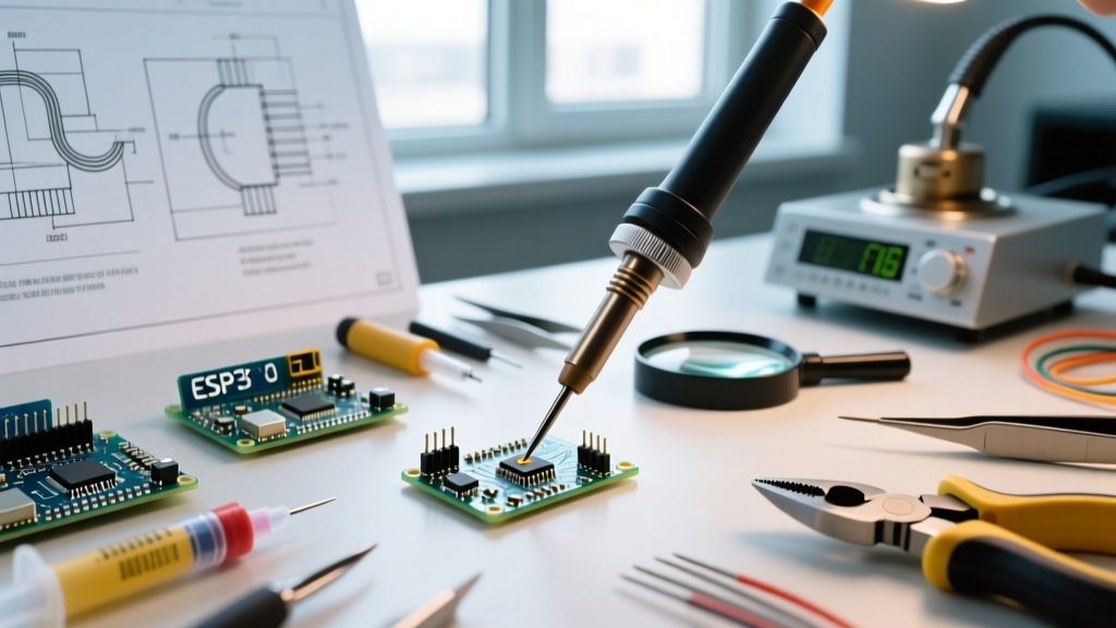
Walk into any electronics lab or browse any DIY forum in 2026, and you will inevitably see beginners purchasing conical soldering tips for fine-pitch printed circuit board (PCB) work. The logic seems sound: a sharper point equals higher precision. However, when it comes to the physics of thermal transfer and the strict requirements of modern lead-free soldering, this assumption is fundamentally flawed. In this comprehensive method comparison, we break down the realities of conical tip soldering versus the industry-standard chisel geometry, examining thermal recovery, surface tension, and IPC-A-610 compliance.
The 'Precision' Trap for Beginners
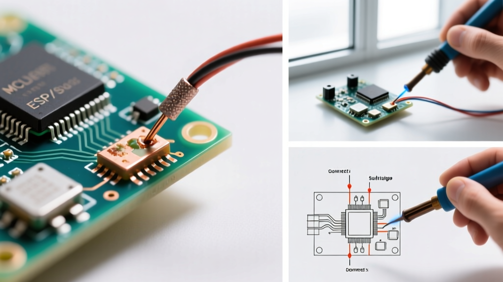
When hobbyists unbox a new station like the Hakko FX-888D (retailing around $115) or the Weller WE1010NA (around $120), the included default tip is almost always a conical shape, such as the Hakko T18-B or the Weller RT1. Manufacturers include these because they are versatile for basic point-to-point wire soldering and look 'professional' to untrained eyes. However, attempting to drag a conical tip across a row of 0.1-inch header pins or an SOIC-8 integrated circuit footprint often results in catastrophic failure modes: cold joints, tombstoning, and lifted pads. To understand why, we must look at the thermodynamics of the soldering iron tip.
Thermal Transfer Physics: Why Geometry Dictates Success
Soldering is not about melting the solder; it is about heating the pad and the component lead simultaneously so the solder can wet the surfaces. The efficiency of this heat transfer is governed by the contact surface area between the tip and the joint.
The Surface Area Rule: A conical tip touches a flat PCB pad at a single, microscopic tangent point. A chisel tip, laid flat, creates a broad rectangular thermal bridge. Even a narrow 1.6mm chisel tip (like the Hakko T18-D16) offers exponentially more surface area contact than a 0.5mm conical needle.
Modern lead-free alloys, such as SAC305 (Sn96.5/Ag3.0/Cu0.5), have a higher melting point (217°C to 220°C) and a narrower plastic range compared to legacy 63/37 leaded eutectic solder. When using a conical tip on a ground plane or a large copper pour, the tiny contact point acts as a thermal bottleneck. The station's heater may push the tip to 380°C, but the heat cannot transfer into the copper fast enough. The operator compensates by pressing harder and dwelling longer, which oxidizes the tip, degrades the flux, and eventually delaminates the PCB pad.
Head-to-Head Comparison Matrix
Below is a direct comparison of the most common tip geometries used in modern electronics rework, highlighting why chisel and bevel shapes dominate professional environments.
| Tip Geometry | Example Model (Hakko / Weller) | Avg. Cost (2026) | Thermal Transfer | Best Application | IPC Compliance Ease |
|---|---|---|---|---|---|
| Conical (Needle) | T18-B / RT1 | $9.50 / $14.99 | Poor (Point contact) | Deep cavity wiring, turret terminals | Difficult |
| Chisel (Flat) | T18-D24 / RT4 | $9.50 / $14.99 | Excellent (Broad contact) | Through-hole, SMD, ground planes | Very High |
| Bevel (Hoof) | T18-C2 / RT8 | $10.50 / $15.99 | Great (Scoop contact) | Drag soldering, large wire lugs | High |
| Knife (K-Type) | T18-K / RT21 | $11.00 / $16.99 | Good (Edge contact) | 0402/0201 SMD, tight pitch QFP | High |
When Conical Tip Soldering Actually Wins
Despite its limitations on flat PCBs, conical tip soldering is not obsolete. It remains the superior method for specific, non-planar applications where a flat chisel edge simply cannot physically reach the joint.
Scenario 1: Turret Terminals and Point-to-Point Wiring
When building tube amplifiers or aerospace point-to-point wiring harnesses, components and wires are wrapped around metal turret stakes. A chisel tip cannot easily maneuver into the narrow crevices between a wrapped 22 AWG wire and the turret wall. A 1.0mm conical tip can penetrate these tight 3D geometries, delivering heat directly to the wire core without shorting against adjacent stakes.
Scenario 2: Deep Cavity Rework and Via Repair
If you are repairing a broken via deep inside a multi-layer board, or soldering a micro-connector recessed inside a 3D-printed or injection-molded enclosure, the sidewalls will block a chisel tip. A long, slender conical tip acts as a thermal probe, reaching down into the cavity to reflow the joint. As noted in Adafruit's Guide to Excellent Soldering, managing heat in confined spaces requires precise tip placement, which is where the needle profile shines.
Executing IPC-Compliant Joints: A Method Comparison
The IPC-A-610 standard for acceptability of electronic assemblies mandates specific wetting angles and fillet shapes. A proper solder joint should exhibit a concave fillet with a wetting angle of less than 90 degrees, resembling a smooth volcano slope.
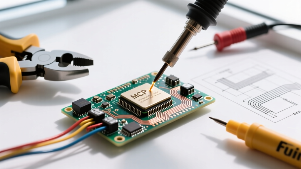
- The Chisel Method (Recommended for PCBs): Place the flat edge of the chisel tip so it simultaneously touches the component lead and the PCB pad. Apply solder to the joint, not the tip. The broad thermal bridge heats both surfaces evenly in 1.5 to 2.5 seconds. The flux activates at 150°C-180°C, cleaning the oxides, and the solder flows via capillary action into the barrel or under the SMD lead.
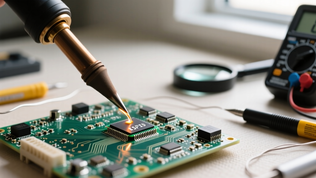
- The Conical Method (High Risk on PCBs): The operator touches the point to the lead. The lead heats up, but the pad remains relatively cool. Solder is applied, but it only wets the lead, forming a convex 'ball' that sits on top of the pad without metallurgical bonding to the copper. This is a classic cold joint, which will inevitably crack under thermal cycling or mechanical vibration.
Troubleshooting Edge Cases and Failure Modes
If you are currently struggling with conical tip soldering on PCBs, you are likely experiencing one of the following failure modes. Here is how to diagnose and fix them without simply turning up the temperature.
Failure Mode: Tombstoning on SMD Components
The Cause: When using a conical tip on 0603 or 0402 surface mount components, the lack of thermal mass means one pad heats significantly faster than the other. The flux on the hotter pad activates and outgases violently, pulling the component upright like a tombstone.
The Fix: Switch to a small chisel tip (e.g., Weller RT3 or Hakko T18-D12). Bridge both the pad and the component termination simultaneously to ensure equal thermal equilibrium before the solder melts.
Failure Mode: Rapid Tip Oxidation (Blackening)
The Cause: Because conical tips transfer heat poorly to large pads, users crank their station to 420°C+ and press down hard. This burns the rosin flux instantly and oxidizes the iron plating on the tip, turning it black and rendering it non-stick.
The Fix: Never exceed 360°C for standard lead-free work. If the joint isn't flowing in 3 seconds, your tip geometry is wrong for the thermal mass of the board. Switch to a larger chisel or bevel tip to increase thermal transfer, rather than increasing the temperature. For a deep dive on tip maintenance, SparkFun's soldering tutorial offers excellent visual guides on tinning and preserving tip life.
Final Verdict: What Should Be in Your Cart?
If your primary work involves printed circuit boards, surface mount devices, or through-hole components on modern FR4 fiberglass, conical tip soldering should be abandoned in favor of chisel or knife geometries. The 'precision' of a conical tip is an optical illusion; true precision in soldering comes from thermal control and wetting dynamics, which require maximum surface area contact.
Keep a single conical tip (like the $9.50 Hakko T18-B) in your toolkit strictly for 3D wiring harnesses, deep cavity repairs, and tight mechanical clearances. For the other 95% of your electronics work, invest in a high-quality set of chisel tips ranging from 1.2mm to 3.2mm. Your joints will flow faster, your pads will remain intact, and your assemblies will effortlessly pass IPC inspection standards.