
The Hidden Financial Drain of Poor Soldering Thermodynamics
When electronics manufacturers, prototyping labs, and serious hobbyists ask, what is the proper heating procedure for soldering, the conversation usually revolves around joint reliability and IPC compliance. However, from a strict cost-analysis perspective, thermal management is fundamentally about protecting your bottom line. In 2026, with the widespread adoption of ultra-dense HDI (High-Density Interconnect) boards and sensitive bottom-terminated components (BTCs), a single thermal misstep can cascade into hundreds of dollars in scrapped materials and diagnostic labor.
Improper heating does not just yield ugly solder joints; it causes invisible micro-fractures, flux burn-off, and pad cratering. To understand the true ROI of proper technique, we must break down the exact procedure, analyze the cost of failure modes, and evaluate the equipment required to execute it profitably.
The Core Question: What Is the Proper Heating Procedure for Soldering?
According to the IPC J-STD-001 requirements for soldered electrical and electronic assemblies, the proper heating procedure is defined by simultaneous thermal elevation of both the pad and the component lead, followed by the introduction of the solder alloy. Let us break this down into a cost-conscious, three-phase workflow.
Phase 1: Tip Selection and Thermal Matching
The most common cost-leak in soldering is using a tip with insufficient thermal mass for the joint, leading the operator to compensate by cranking the station temperature to 400°C (752°F). This causes rapid tip oxidation. A standard lead-free compatible tip (e.g., Hakko T18 series) costs around $7. When abused with excessive heat, its lifespan drops from months to days, adding hundreds of dollars in annual consumable costs per workstation.
- Rule: Select the largest tip geometry that fits the pad. For a 0805 SMD component, use a 1.6mm chisel. For a heavy ground-plane through-hole pin, use a 5mm bevel or knife tip.
- Cost Impact: Correct tip matching reduces dwell time by up to 60%, preserving both the tip's iron plating and the PCB's FR-4 substrate.
Phase 2: Simultaneous Pad and Lead Heating
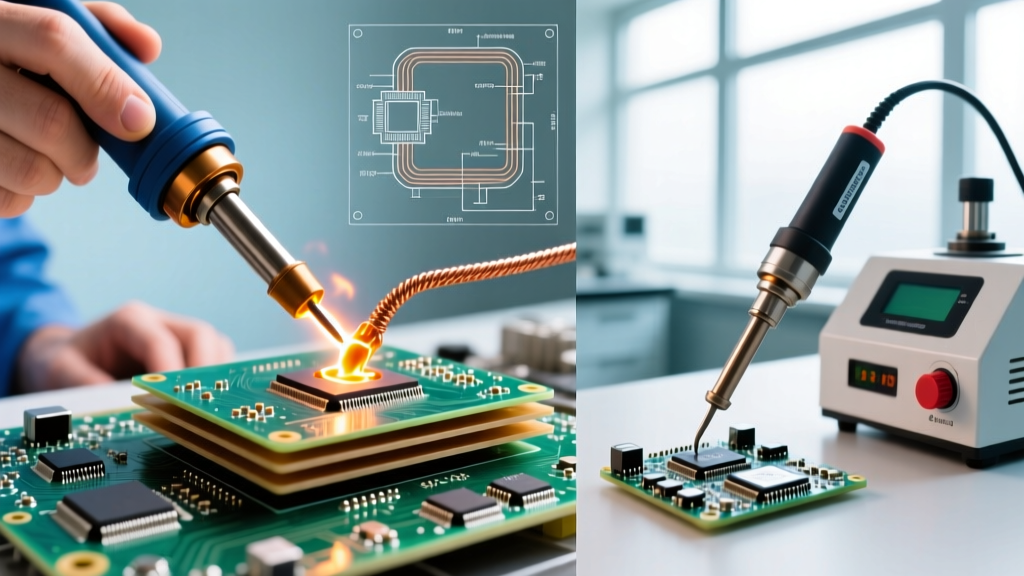
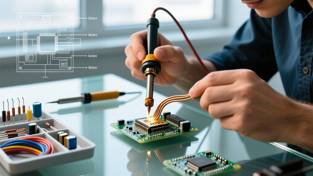
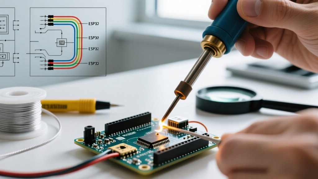
The golden rule of soldering is to heat the joint, not the solder. The iron tip must physically bridge the component lead and the PCB pad simultaneously for 1 to 1.5 seconds before any solder wire is introduced.
Warning: Feeding solder directly onto the iron tip and 'transferring' it to the joint creates a cold solder joint. The flux burns off during the transfer, and the thermal energy is insufficient to form a proper intermetallic compound (IMC) layer. Reworking a single cold joint on a 4-layer board costs an average of $35 in labor and flux/consumables.
Phase 3: Solder Application and the 3-Second Dwell Limit
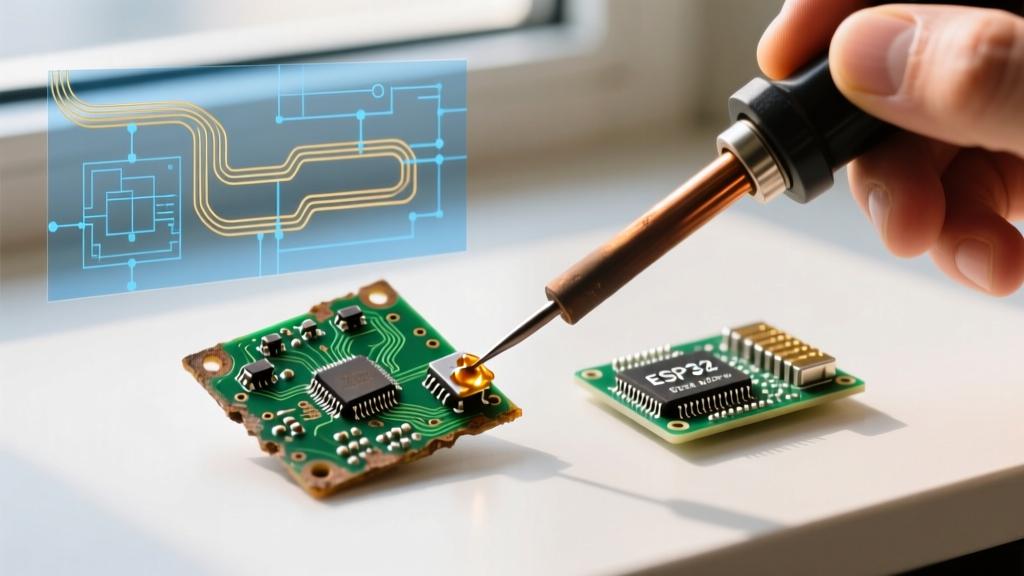
Once the joint reaches the melting point of the alloy (typically 217°C for SAC305 lead-free solder), apply the solder wire to the joint, not the tip. The total time the iron is in contact with the pad should never exceed 3 seconds. As outlined in the NASA-STD-8739.3 Workmanship Standard, prolonged heating causes the copper pad to separate from the fiberglass substrate, a catastrophic failure known as pad lift.
Cost Analysis: The Price of Thermal Mismanagement
To illustrate why mastering the proper heating procedure is a financial imperative, consider the Cost of Poor Quality (COPQ) associated with common thermal errors in a mid-volume prototyping environment.
| Heating Error | Resulting Defect | Direct Material Cost | Rework / Labor Cost |
|---|---|---|---|
| Excessive Dwell Time (>4s) | Pad Delamination / Lift | $15 - $150 (Scrapped PCB) | $65+ (Wire-jump repair) |
| Insufficient Pre-heat | MLCC Flex / Thermal Shock Cracking | $0.50 - $5.00 (Capacitor) | $120+ (X-Ray & Diagnostic) |
| Transferring Solder (Cold Joint) | High-Resistance Intermittent Fault | $0 (Solder) | $85+ (Field Return / RMA) |
| Overheating Flux | Corrosive Residue / Dendrite Growth | $0 | $40 (Ultrasonic Cleaning) |
Equipment ROI: Can Cheap Irons Deliver the Proper Procedure?
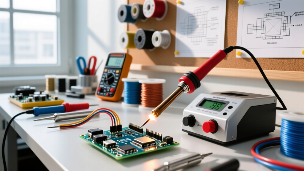
Executing the correct heating procedure requires an iron with high thermal recovery rates. When the cold solder wire touches the heated joint, the tip temperature plummets. A smart station must inject massive current into the heater element to recover that heat within milliseconds, preventing the operator from holding the iron in place too long.
Station Comparison Matrix (2026 Market Pricing)
- Pine64 Pinecil V2 ($26): Excellent for lightweight SMD work and hobbyists. However, its 65W max output and lightweight tip mass struggle with multi-layer ground planes. ROI Verdict: High risk of thermal starvation on heavy copper, leading to potential board damage.
- Hakko FX-951 ($265): The industry workhorse. Uses composite cartridge tips with the heater embedded directly inside the tip. Recovers heat in under 1.5 seconds. ROI Verdict: Pays for itself after preventing just three scrapped prototype boards.
- JBC CD-2B ($680): Features an advanced thermal management system that detects when the tip touches a pad and pre-emptively surges power. Unmatched for BTCs and heavy thermal mass. ROI Verdict: Essential for high-density commercial labs; reduces rework time by an estimated 40%.
Component-Specific Thermal Limits and Edge Cases
Understanding what is the proper heating procedure for soldering also means recognizing that different components have vastly different thermal tolerances. Blindly applying a 350°C profile across the board is a recipe for financial loss.
Multilayer Ceramic Capacitors (MLCCs)
MLCCs are highly susceptible to thermal shock. If a 380°C iron tip touches a cold ceramic body, the rapid localized expansion can cause microscopic cracks. These cracks may not fail during initial QA testing but will lead to short circuits in the field months later. Solution: Use a pre-heating mat (set to 100°C) to reduce the thermal delta before applying the iron.
Bottom-Terminated Components (QFN/DFN)
You cannot properly solder the exposed thermal pad of a QFN chip using only a hand iron. Attempting to flood the side leads with excess solder to 'wick' underneath results in bridging and insufficient thermal transfer. Solution: The proper procedure dictates using a hot air rework station (e.g., Quick 861DW at $160) with a custom stencil to apply solder paste to the pad, followed by a controlled 240°C hot-air profile.
Summary: Technique as a Cost-Control Mechanism
Ultimately, the proper heating procedure is not just an academic exercise in metallurgy; it is a vital cost-control mechanism. By matching tip geometry to thermal mass, enforcing the simultaneous heating rule, and respecting the 3-second dwell limit, you eliminate the root causes of 80% of all soldering-related rework. For further reading on advanced alloy profiles and flux chemistries, consult the technical documentation provided by Indium Corporation. Investing in a high-recovery soldering station and training operators on strict thermal discipline will yield an immediate, measurable reduction in your scrap and RMA budgets.