
The Reality of Ultrasonic Imaging with Arduino
When most hobbyists hear 'ultrasonic sensor,' they immediately think of the HC-SR04—a $2 module perfectly capable of measuring distance to a nearby wall. However, ultrasonic imaging (such as acoustic microscopy, non-destructive testing, or low-frequency medical sonography) is an entirely different discipline. It requires capturing high-frequency acoustic echoes, resolving microvolt-level return signals, and performing real-time beamforming.
A standard Arduino Uno (ATmega328P) maxes out at a 15 kSPS ADC sampling rate with 10-bit resolution. To image a 2.25 MHz acoustic wave, the Nyquist theorem dictates you need an Analog-to-Digital Converter (ADC) sampling at a minimum of 10 MSPS, though 40 to 80 MSPS is preferred for envelope detection and phase coherence. Therefore, when we discuss an ultrasonic imaging Arduino setup, we are strictly referring to the Arduino IDE ecosystem powering high-performance microcontrollers like the Teensy 4.1 (600 MHz Cortex-M7) or the Arduino Portenta H7, paired with a dedicated Ultrasound Analog Front End (AFE).
Expert Note: Never attempt to route raw 50 MHz ultrasound RF signals directly into a microcontroller's GPIO. The parasitic capacitance and digital noise floor will obliterate the acoustic echo data. You must use a dedicated AFE.
Datasheet Deep Dive: Analog Devices AD9278
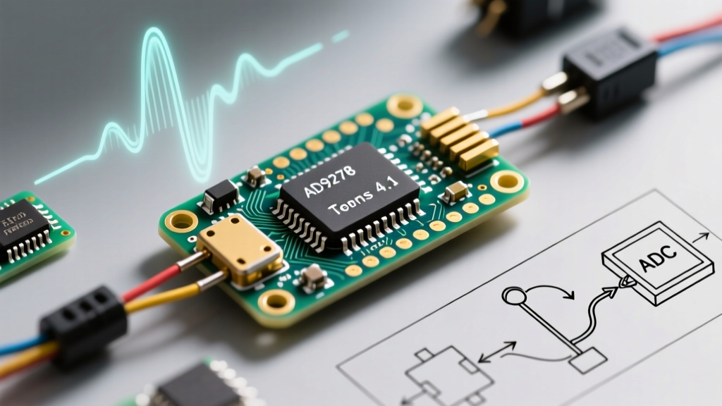
For this explainer, we are bypassing the popular AD9271. Why? The AD9271 utilizes LVDS (Low-Voltage Differential Signaling) for its data outputs. While excellent for FPGAs, interfacing LVDS with a Teensy 4.1 requires external translator ICs (like the TI SN65LVDS34), adding severe routing complexity and jitter. Instead, we turn to the Analog Devices AD9278, an octal 12-bit, 80 MSPS ultrasound AFE that features a parallel CMOS output bus, making it vastly more compatible with high-speed ARM Cortex-M7 FlexIO peripherals.
Chasing the Microvolt Echo: LNA and PGA Stages
Acoustic waves attenuate rapidly in tissue or dense materials (often exceeding 1 dB/cm/MHz). By the time an echo returns to a 2.25 MHz PZT transducer, the signal may be as low as 10 µV. The AD9278 handles this via a three-stage amplification pipeline detailed in Section 4 of its datasheet.
| AFE Stage | Datasheet Parameter | Spec Value | Imaging Impact |
|---|---|---|---|
| LNA (Low Noise Amp) | Input Voltage Noise | 0.7 nV/√Hz | Resolves deep-tissue micro-calcifications without adding thermal noise. |
| LNA | Gain Options | 19 dB / 24 dB | Fixed front-end gain to establish a strong baseline Signal-to-Noise Ratio (SNR). |
| PGA (Variable Gain) | Dynamic Range | 24 dB to 42 dB | Time-Gain Compensation (TGC). Increases gain as deeper echoes return. |
| Anti-Alias Filter | Cutoff Frequency | Programmable (10-70 MHz) | Prevents high-frequency harmonic noise from folding into the ADC baseband. |
The 12-Bit, 80 MSPS ADC Core & CMOS Multiplexing
The AD9278 integrates eight 12-bit ADCs. At 80 MSPS, the raw data rate for eight channels would require 96 parallel data pins (8 channels × 12 bits). To prevent a PCB routing nightmare, the datasheet specifies a multiplexed parallel CMOS interface. The AFE outputs data from two channels per clock cycle over a 24-bit bus, utilizing a 4x or 2x clock multiplier. This reduces the physical pin count on the Teensy 4.1, allowing you to route the data into the MCU's parallel camera interface (CSI) or FlexIO shift registers.
Hardware Integration: Wiring to the Teensy 4.1
Interfacing this AFE requires strict adherence to the datasheet's timing diagrams. Below is the step-by-step initialization sequence using the Arduino IDE (via Teensyduino).
- SPI Configuration: The AD9278 uses a 3-wire SPI bus for register configuration. Initialize the SPI bus at 20 MHz (CPOL=0, CPHA=0). Do not exceed 20 MHz, or the internal PLL lock bits may fail to write.
- Enable the LNA: Write
0x18to Register0x02to power up the LNA and set the gain to 24 dB. - Configure TGC (Time-Gain Compensation): Use the SPI to set the PGA slope. For a 5 cm imaging depth in water (1500 m/s), the round-trip time is ~66 µs. Map the PGA gain from 24 dB at t=0 to 40 dB at t=66 µs via the internal DAC control registers.
- FlexIO Setup: Configure the Teensy 4.1 FlexIO module to trigger on the AFE's
DCO(Data Clock Output). Set the FlexIO shifters to pack the 24-bit multiplexed CMOS words into 32-bit integers in the MCU's DMA buffer.
Edge Cases & Failure Modes in Prototyping
Building an ultrasonic imaging Arduino prototype is fraught with analog physics traps that the datasheet only hints at. Be prepared for the following failure modes:
1. Acoustic Impedance Mismatch
The AD9278 LNA expects a specific source impedance to maintain its 0.7 nV/√Hz noise figure. If you wire a raw 2.25 MHz piezoelectric transducer (which can have a capacitive reactance of -j150Ω at resonance) directly to the LNA without an LC matching network, you will suffer massive signal reflection at the PCB trace. Solution: Design a Pi-network matching circuit to transform the transducer's impedance to the AFE's optimal 50Ω to 100Ω differential input range.
2. Thermal Throttling on the AFE
Eight simultaneous ADC channels sampling at 80 MSPS generate significant heat. The AD9278 datasheet notes a typical power dissipation of 1.4W. In a 2026 compact 3D-printed probe enclosure, this will raise the junction temperature past 85°C within 12 minutes, triggering the internal thermal shutdown bit (Register 0x0F). Solution: You must expose the thermal pad on the bottom of the QFN package to a multi-layer copper pour, and ideally attach a 10mm x 10mm aluminum heatsink with thermal interface tape.
3. Ground Bounce on the CMOS Bus
When all 24 CMOS output pins switch simultaneously from HIGH to LOW, the transient current spike causes 'ground bounce,' corrupting the least significant bits (LSBs) of your 12-bit ADC data. This manifests as horizontal banding noise in your B-mode ultrasound images. Solution: Enable the AD9278's internal 'Staggered Output' mode via SPI Register 0x14. This offsets the switching times of the even and odd data pins by 1 ns, flattening the current draw profile.
2026 Prototype BOM & Cost Breakdown
Transitioning from basic distance sensors to true acoustic imaging requires a realistic budget. Below is the estimated cost for a single-channel 8-element phased array prototype built in 2026.
| Component Category | Specific Model / Part | Est. 2026 Price |
|---|---|---|
| Ultrasound AFE | AD9278BSTZ (Raw IC) | $52.00 |
| Microcontroller | PJRC Teensy 4.1 (Cortex-M7) | $84.95 |
| Transducer Array | 8x 2.25 MHz PZT Elements (Custom cut) | $120.00 |
| Pulser / HV Switch | MAX4940 (High-Voltage TX/RX Switch) | $14.50 |
| PCB Fabrication | 4-Layer Impedance Controlled (JLCPCB) | $45.00 |
| Total Prototype Cost | Excluding assembly and scope | ~$316.45 |
Frequently Asked Questions
Can I use a standard Arduino Uno for ultrasonic imaging?
No. The ATmega328P lacks the sampling speed, memory bandwidth, and parallel interfaces required to capture RF ultrasound data. You must use an Arduino IDE-compatible 32-bit ARM processor like the Teensy 4.1 or Arduino Portenta H7.
What software is used for beamforming on the MCU?
While the Teensy 4.1 can perform basic delay-and-sum (DAS) beamforming using its floating-point unit (FPU) and NEON-like DSP instructions, most developers stream the raw DMA buffers via USB 3.0 or Ethernet to a host PC running Python (NumPy/SciPy) or CUDA for real-time B-mode image reconstruction.
How do I generate the high-voltage transmit pulse?
The AD9278 is strictly a receiver (AFE). To transmit the acoustic ping, you need a high-voltage pulser circuit (often 50V to 100V) utilizing MOSFETs or dedicated ultrasound transmit ICs like the Texas Instruments TX734, triggered by a separate GPIO pin on the Teensy.