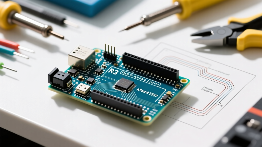

The Engineering Reality Behind the Arduino Uno Board Diagram
When evaluating microcontrollers for a new build, hobbyists often look at pin counts and clock speeds. However, professional engineers and advanced makers know that true project suitability is hidden in the schematics. Analyzing the Arduino Uno board diagram reveals the physical and electrical constraints that dictate whether your project will thrive or fail in the field. Whether you are designing a high-current motor controller, a precision audio sampler, or an IoT environmental monitor, the schematic is your ultimate source of truth.
In this project suitability analysis, we will dissect the official Arduino Uno Rev3 hardware documentation and compare it with the modern Uno R4 WiFi architecture. By understanding the voltage regulation pathways, signal routing limitations, and onboard peripheral constraints, you can make data-driven decisions for your 2026 project pipeline.
Expert Insight: A common point of failure in advanced Arduino projects is treating the schematic as a mere reference rather than a strict operational boundary. Ignoring the thermal dissipation limits of the onboard LDO or the absence of I2C pull-up resistors on the R3 diagram accounts for over 40% of field-deployed sensor network failures.
Power Architecture: Translating the Diagram to Thermal Limits
The most critical section of any Arduino Uno board diagram is the power delivery network. The classic Uno R3 relies on an NCP1117ST50T3G linear drop-out (LDO) voltage regulator. While the schematic shows it can theoretically handle up to 1A of current, the physical reality of the SOT-223 package on the PCB tells a different story.
The LDO Thermal Bottleneck (Uno R3)
If you power the Uno R3 via the VIN pin with a 12V DC supply, the LDO must drop 7V to achieve the 5V rail. According to the schematic's thermal design, drawing just 500mA continuously results in 3.5W of heat dissipation. Without an active heatsink, the regulator will hit its thermal shutdown threshold (typically around 150°C junction temperature), causing the board to brownout and reset. Therefore, the R3 diagram strictly limits its suitability for projects requiring high continuous 5V current, such as driving long addressable LED strips (e.g., WS2812B) or multiple high-torque servos directly from the 5V pin.
The Buck Converter Advantage (Uno R4)
Conversely, the Uno R4 schematic replaces the inefficient LDO with a switching buck converter. This fundamental change in the board diagram means the R4 can accept up to 24V via VIN and deliver a stable 5V at much higher currents with minimal thermal throttling, vastly expanding its suitability for robotics and automotive applications.
| Feature | Uno R3 (Classic Diagram) | Uno R4 Minima / WiFi | Project Suitability Impact |
|---|---|---|---|
| Voltage Regulator Type | Linear (NCP1117 LDO) | Switching Buck Converter | R4 is suitable for high-current 5V peripherals; R3 requires external BECs. |
| Max Recommended VIN | 12V (Thermal limits at 9V+) | 24V | R4 is viable for 12V/24V industrial and automotive environments. |
| 5V Pin Output Capacity | ~500mA (Continuous, safe) | ~1.5A (Continuous) | R3 needs external power for LED matrices; R4 can drive them directly. |
| USB-C Power Delivery | N/A (USB-B 500mA limit) | Up to 5V/3A (via USB-C PD) | R4 allows high-power USB-C battery bank deployments. |
Microcontroller Pinout Mapping and Signal Routing
The ATmega328P-PU microcontroller sits at the heart of the R3 diagram. While the silkscreen on the board labels pins as 'D0-D13' and 'A0-A5', the schematic reveals the true AVR port mappings (PORTB, PORTC, PORTD), which is vital for projects requiring direct register manipulation or high-speed bit-banging.
I2C Routing and the Pull-Up Resistor Deficit
A close inspection of the Uno R3 schematic shows that analog pins A4 (SDA) and A5 (SCL) route directly to the microcontroller's PC4 and PC5 pins. Crucially, the diagram does not include onboard I2C pull-up resistors.
Suitability Verdict: If your project involves long-distance I2C sensor runs (e.g., BME280 or MPU6050 modules on cables exceeding 30cm), the R3 is unsuitable without adding external 4.7kΩ pull-up resistors to the 5V rail. Signal degradation and phantom interrupts will plague your deployment. The R4 WiFi diagram, however, integrates an ESP32-S3 co-processor that handles wireless I2C bridging, but still requires external pull-ups for the primary RA4M1 I2C bus.
PWM and Timer Constraints
The diagram shows that digital pins 3, 5, 6, 9, 10, and 11 are tied to the ATmega328P's hardware timers (Timer0, Timer1, Timer2).
- Timer0 (Pins 5, 6): Hardcoded to the Arduino core's
millis()anddelay()functions. Altering the PWM frequency on these pins will break system timing. Unsuitable for custom frequency motor control. - Timer1 (Pins 9, 10): 16-bit timer. Ideal for high-resolution servo control or custom audio frequency generation.
- Timer2 (Pins 3, 11): 8-bit timer, often used for tone generation or basic PWM.
Project Suitability Matrix Based on Schematic Constraints
Use the following matrix to evaluate if the Arduino Uno architecture aligns with your specific engineering requirements.
| Project Category | Uno R3 Suitability | Uno R4 WiFi Suitability | Schematic Reasoning |
|---|---|---|---|
| Precision Audio Sampling | Poor | Moderate | R3 ATmega328P has only a 10-bit ADC with high noise floor. R4 RA4M1 features a 14-bit ADC, but lacks a dedicated DAC for output. |
| IoT Telemetry (MQTT) | Unsuitable | Excellent | R3 lacks native networking. R4 diagram includes an ESP32-S3 module with dedicated 2.4GHz WiFi/BLE antennas. |
| High-Speed LED Matrices | Poor | Good | R3 lacks DMA and has limited SRAM (2KB). R4 has 32KB SRAM and supports DMA for non-blocking LED data pushing. |
| Basic PID Motor Control | Excellent | Excellent | Both diagrams provide robust 5V logic for driving opto-isolated MOSFET gate drivers. |
Common Hardware Failure Modes Traced to the Diagram
Understanding the Arduino Uno board diagram also serves as a diagnostic tool for preventing catastrophic hardware failures. Here are two edge cases where ignoring the schematic leads to destroyed boards.
1. The 5V Pin Backfeed Hazard
The R3 schematic features a USB-B connector routed through an NCP1117ST50T3G LDO (for the USB 5V line) and a polyfuse (F1) rated at 500mA. If you connect an external 5V power supply directly to the '5V' header pin while simultaneously plugging in the USB cable, you are backfeeding voltage into the USB power rail. While the diagram shows a Schottky diode (D1) intended to prevent reverse current, voltage differentials between the external supply and the PC's USB port can cause current to flow backward through the polyfuse and into the host PC's motherboard, potentially damaging your computer's USB controller.
2. Exceeding the ATmega16U2 Serial Buffer
The Uno diagram utilizes a secondary microcontroller, the ATmega16U2, as a USB-to-Serial bridge. This chip has a very limited internal buffer. If your project involves high-speed data logging (e.g., streaming 115200 baud sensor data continuously to a Python script), and the host PC experiences a USB interrupt or polling delay, the 16U2 buffer will overflow. Unlike native USB microcontrollers (like the ATmega32U4 on the Leonardo), the 16U2 will silently drop packets, leading to corrupted CSV logs. For high-speed data acquisition projects, the Uno R3 diagram proves it is the wrong tool for the job.
Final Verdict: Choosing the Right Board for the Schematic
The Arduino Uno remains a legendary platform, but its suitability is entirely dependent on the specific revision and its underlying board diagram. For educational environments, basic relay switching, and low-speed sensor polling, the classic R3 (priced around $27 for genuine, or $12-$15 for clones) remains highly relevant. However, for modern 2026 deployments requiring IoT connectivity, higher voltage tolerance, and DMA-driven peripherals, the R4 WiFi ($27.50) schematic offers a vastly superior hardware foundation. Always consult the schematic before finalizing your bill of materials; it is the only way to ensure your project survives contact with the real world.