
The Evolution of USB-C Charging: SPR vs. EPR in 2026
Designing a custom power delivery system requires more than just connecting positive and negative terminals. As of 2026, the USB-C ecosystem has fully transitioned into the USB Power Delivery 3.1 specification, dividing the landscape into Standard Power Range (SPR, up to 100W) and Extended Power Range (EPR, up to 240W). When engineers and DIY enthusiasts search for a USB C wiring diagram for charging, they are often unprepared for the strict configuration channel (CC) requirements and high-current trace routing necessary to safely negotiate these power contracts.
This step-by-step walkthrough focuses on wiring a 16-pin or 24-pin USB-C female receptacle (UFP/Sink) for a custom battery pack, solar charge controller, or high-power DIY project. We will cover the exact pinouts, necessary pull-down resistors, wire gauge selections, and soldering techniques required to pass a 100W+ power contract without triggering thermal throttling or catastrophic failure.
Understanding the USB-C Receptacle Pinout
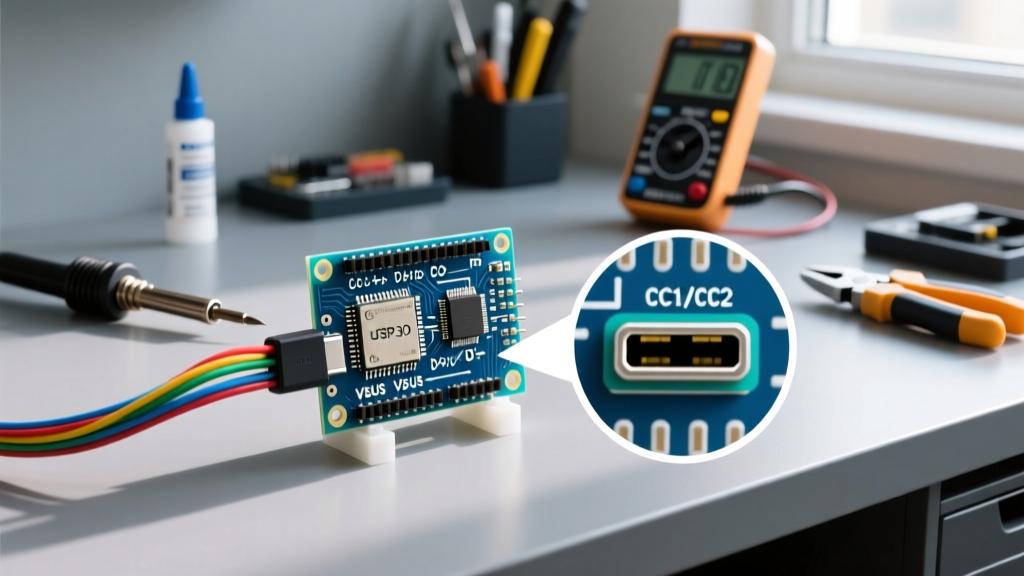
Unlike legacy USB-A or Micro-B connectors, USB-C utilizes a symmetrical 24-pin layout (often simplified to 16 pins on DIY breakout boards). For a pure charging application, the SuperSpeed data lanes (TX/RX) can be ignored, but the VBUS, GND, and CC pins are non-negotiable. Below is the critical pinout mapping for a charging sink.
| Pin Name | Function | Wire Gauge / Trace Spec | Notes for Charging Sink (UFP) |
|---|---|---|---|
| VBUS (A4, B9, etc.) | Power Delivery (5V - 48V) | 20 AWG (Wire) / 50mil 2oz (Trace) | Must handle up to 5A continuous. Parallel pins on 24-pin connectors. |
| GND (A1, B12, etc.) | Ground Return | 20 AWG (Wire) / 50mil 2oz (Trace) | Parallel routing required to minimize voltage drop and inductance. |
| CC1 (A5) | Configuration Channel 1 | 28 AWG (Wire) / 10mil (Trace) | Requires 5.1kΩ pull-down to GND for UFP identification. |
| CC2 (B5) | Configuration Channel 2 | 28 AWG (Wire) / 10mil (Trace) | Requires 5.1kΩ pull-down to GND for reversible plug support. |
| D+ / D- | USB 2.0 Data | 28 AWG (Shielded Pair) | Used for legacy BC 1.2 / QC 3.0 fallback if PD negotiation fails. |
Essential Tools and Materials
High-current USB-C wiring demands precision. Cold solder joints on VBUS pins will result in severe voltage drops, causing the PD controller to reject the 5A contract. Gather the following before beginning:
- USB-C 16-Pin or 24-Pin Mid-Mount Receptacle: Choose a mid-mount (dip-style) PCB footprint for superior mechanical shear strength compared to surface-mount (SMD) edge connectors.
- Wire: 20 AWG silicone-jacketed wire for VBUS/GND (rated for 200°C and 5A+). 28 AWG for CC and data lines.
- Resistors: Two 5.1kΩ (±1% tolerance) 0805 SMD resistors. Do not use 5% tolerance carbon film; PD controllers may misread the voltage drop.
- Soldering Equipment: Temperature-controlled station set to 360°C (for lead-free) or 330°C (for 63/37 Sn/Pb). Use a chisel tip (e.g., Hakko T18-D24) for high thermal transfer to ground planes.
- Flux: Amtech NC-559-V2-TF or ChipQuik TACKY FLUX. No-clean rosin flux is mandatory for the CC pins to prevent parasitic leakage currents.
Step-by-Step Wiring Walkthrough
Step 1: PCB Preparation and CC Resistor Placement
Before attaching any wires, the Configuration Channel (CC) must be established. The USB Implementers Forum (USB-IF) strictly mandates that a Sink (UFP) must present a 5.1kΩ pull-down resistor on both CC1 and CC2 to ground. Without these resistors, a standard USB-C PD wall charger will output exactly 0V.
- Apply a micro-dot of tacky flux to the CC1 and CC2 pads on your breakout board.
- Place the 5.1kΩ 0805 resistors using precision tweezers.
- Tack solder one side, verify alignment, and flow solder on the other. Ensure no solder bridges to the adjacent high-speed data lanes, as this will cause a short to ground and disable the port.
Step 2: Soldering the VBUS and GND High-Current Paths
In a 100W SPR setup (20V @ 5A), the VBUS and GND lines carry significant thermal loads. If your custom wiring harness exceeds 6 inches in length, voltage drop becomes a critical factor.
- Strip exactly 3mm of insulation from your 20 AWG VBUS (Red) and GND (Black) wires.
- Pre-tin the wires and the receptacle pads separately. Do not attempt to heat the wire and pad simultaneously; the large ground planes on USB-C receptacles act as massive heatsinks and will wick heat away, resulting in a cold joint.
- Apply generous flux to the VBUS pads. Bring the pre-tinned wire to the pad and apply the iron for 2-3 seconds until the solder flows smoothly into a concave fillet, conforming to IPC-A-610 Class 2 soldering standards.
- Repeat for the GND pins. If using a 24-pin connector, parallel the A1/A12 and B1/B12 ground pins together using a single 20 AWG wire or a heavy copper braid to halve the resistance.
Step 3: Wiring the Data Lines for Legacy Fallback
While PD negotiation happens over the CC lines, many older power banks and car chargers rely on the D+ and D- lines for Quick Charge (QC 2.0/3.0) or Apple 2.4A charging protocols.
- Solder your 28 AWG shielded twisted pair to the D+ (A6) and D- (A7) pins.
- Ensure the shielding drain wire is routed to the connector's metal shell (GND), not to the signal ground, to prevent high-frequency noise from disrupting the CC logic analyzer during handshake.
Step 4: Mechanical Strain Relief and Encapsulation
USB-C connectors are notorious for failing at the wire-to-board junction due to mechanical leverage. After electrical continuity is verified with a multimeter, apply a two-part marine-grade epoxy or UV-curable solder mask over the VBUS and GND wire joints. This prevents wire fatigue and protects against humidity-induced galvanic corrosion, which is especially vital in outdoor solar or automotive applications.
Expert Warning on EPR (Extended Power Range): If your 2026 project utilizes the new PD 3.1 EPR standard (28V, 36V, or 48V at 5A), standard PVC wire insulation is insufficient due to the risk of dielectric breakdown and thermal melting. You must use PTFE (Teflon) or high-temperature silicone insulated wire rated for at least 300V dielectric strength, even if the operating voltage is only 48V, to ensure safety margins against transient inductive spikes.
Common Failure Modes and Troubleshooting
Even with a perfect schematic, physical wiring introduces variables. Consult this diagnostic matrix if your custom USB-C charging port fails to negotiate power:
1. Charger Plugged In, But Output is 0V
Cause: Missing or open-circuit 5.1kΩ pull-down resistors on CC1/CC2.
Solution: The source (DFP) does not recognize a sink is attached. Measure the resistance from CC1 to GND and CC2 to GND with the power disconnected. It must read exactly 5.1kΩ. If it reads infinite, reflow your SMD resistors.
2. Charger Defaults to 5V / 500mA (Ignores 20V/100W Request)
Cause: Voltage drop on the CC lines due to undersized wire or flux residue.
Solution: The PD controller reads the CC voltage to determine the Rp/Rd resistor divider. If flux residue creates a parasitic parallel resistance, the voltage drops below the threshold for a 3A/5A advertisement. Clean the board with 99% isopropyl alcohol and an ESD-safe brush.
3. Intermittent Disconnects Under High Load
Cause: Thermal expansion breaking a marginal VBUS solder joint.
Solution: At 5A, a poor solder joint will heat up, expand, and break the electrical connection, causing the device to reboot. Inspect the VBUS fillets under a magnifying loupe. A good joint is shiny and concave; a bad joint is dull, convex, or cracked. For advanced designs, refer to the STMicroelectronics USB Type-C Design Center for integrated load-switch PCB layouts that mitigate thermal hotspots.
Frequently Asked Questions (FAQ)
Can I wire a USB-C port without a dedicated PD controller IC?
Yes, but only for fixed-voltage, non-negotiated charging. By hardwiring the 5.1kΩ pull-down resistors, a standard PD wall charger will safely output 5V up to 3A (15W). To request 9V, 12V, 15V, or 20V, you must integrate a PD sink controller IC (such as the STUSB4500 or CH224K) that actively communicates over the CC lines.
Do I need to wire all four VBUS pins on a 24-pin connector?
For currents exceeding 3A, absolutely. Paralleling the VBUS (A4, A9, B4, B9) and GND (A1, A12, B1, B12) pins reduces the contact resistance and distributes the thermal load across the PCB. Failing to parallel these pins at 5A will cause the connector housing to melt over time.
What happens if I swap D+ and D-?
USB 2.0 data is half-duplex and differential. Swapping D+ and D- will prevent legacy data communication and break Quick Charge (QC) voltage negotiation, but it will not damage the hardware. USB-C PD negotiation relies solely on the CC pins, so PD charging will still function normally if D+/D- are swapped or omitted entirely.