
The Hidden Cost of Incorrect PCB Soldering Temperatures
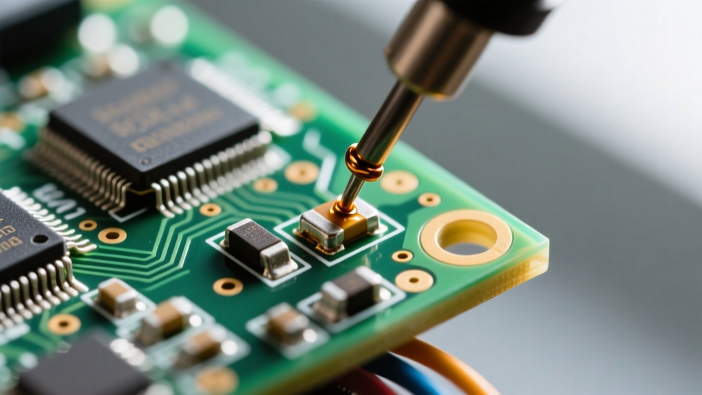
In modern electronics manufacturing and DIY prototyping, dialing in the exact soldering temperature for PCB assemblies is the difference between a reliable circuit and a scrap board. As component densities increase and 0201 passives become standard in 2026 consumer devices, thermal mismanagement doesn't just cause ugly joints—it induces catastrophic micro-cracking in Multi-Layer Ceramic Capacitors (MLCCs) and delaminates FR-4 substrate layers. This troubleshooting guide moves beyond basic tutorials to diagnose, isolate, and fix temperature-related soldering defects using industry-standard methodologies.
Thermal Mass vs. Setpoint: The Core Misconception
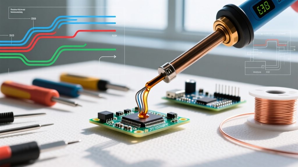
The most common mistake technicians make is confusing the station's setpoint temperature with the actual temperature at the solder joint. According to Hakko's official thermal guidelines, a soldering iron set to 350°C does not instantly transfer 350°C to the pad. The iron must overcome the thermal mass of the component lead, the PCB pad, and the internal copper planes. If your station lacks the wattage to recover quickly (e.g., a standard 40W iron on a heavy ground plane), the tip temperature plummets upon contact, resulting in a cold joint even if the dial reads 380°C.
Diagnostic Matrix: Identifying Temperature-Related Defects
Use this matrix to reverse-engineer the failure mode based on visual inspection under a 10x to 30x stereo microscope.
| Defect Type | Visual Symptom | Root Cause | Corrective Action |
|---|---|---|---|
| Cold Solder Joint | Dull, grainy, or bulbous appearance; poor wetting on the pad. | Iron setpoint too low, or thermal recovery failure due to high ground-plane mass. | Increase setpoint by 20°C; switch to a wider chisel tip (e.g., 2.4mm) to maximize surface contact. |
| Scorched Flux / Burnt Pads | Blackened, carbonized flux residue; pad lifting or discoloration of the solder mask. | Excessive temperature (>400°C) or dwell time exceeding 5 seconds per IPC-A-610 standards. | Lower temperature; use a high-activity no-clean flux to accelerate wetting and reduce dwell time. |
| Solder Balling / Splatter | Micro-spheres of solder scattered around the joint or on adjacent traces. | Moisture in the flux boiling violently due to an overly aggressive initial heat spike. | Pre-heat the PCB to 100°C; apply iron to the pad first, then feed solder wire to buffer the heat. |
| MLCC Flex Cracking | Invisible to naked eye; causes short circuits or capacitance loss. Visible via X-ray or cross-section. | Thermal shock from touching a cold component body with a 380°C tip. | Never touch the ceramic body. Heat the pad only, or use a board preheater for large ceramic components. |
Alloy-Specific Baselines: Setting Your Station
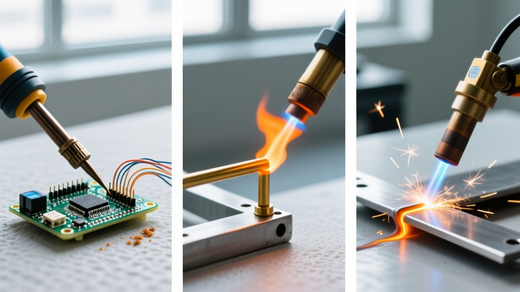
The ideal soldering temperature for PCB work is entirely dependent on the metallurgy of your solder wire. Using lead-free parameters on leaded solder will destroy your tips and burn your flux instantly.
- Sn63/Pb37 (Leaded Eutectic): Melts at 183°C. Recommended Station Setpoint: 320°C - 350°C. This remains the gold standard for DIY, aerospace, and repair work due to its forgiving wetting characteristics and distinct eutectic phase transition.
- SAC305 (Lead-Free): Melts at 217°C. Recommended Station Setpoint: 350°C - 380°C. Requires a station with high thermal recovery (like the Weller WE1010 or Hakko FX-951) because SAC305 has a higher surface tension and resists flowing into plated through-holes (PTH).
- Sn42/Bi57 (Low-Temperature Bismuth): Melts at 138°C. Recommended Station Setpoint: 250°C - 280°C. Ideal for 2026-era IoT repairs and heat-sensitive flex-PCBs. Caution: Bismuth joints are brittle and must never be mixed with leaded solder, which creates a low-melting-point quaternary eutectic that fails at room temperature.
Step-by-Step Troubleshooting Workflow
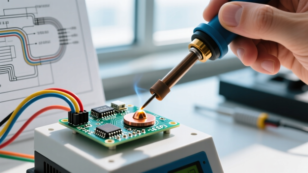
When you encounter a defective joint, do not simply hold a hotter iron to it longer. Follow this systematic rework procedure aligned with IPC J-STD-001 workmanship requirements.
- Assess the Thermal Environment: Is the joint connected to a large copper pour? If yes, apply Kapton tape (polyimide) to surrounding sensitive components to protect them from the increased heat required.
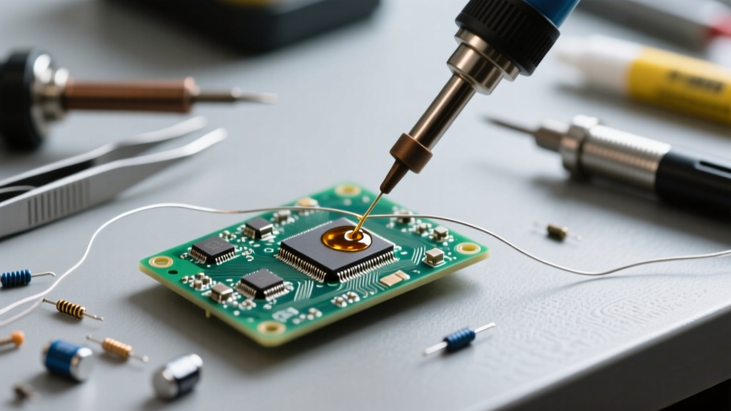
- Chemical Preparation: Apply a generous amount of high-quality tack flux (e.g., Amtech NC-559-V2-TF or Chip Quik SMD291AX). Flux lowers the surface tension of the solder and acts as a thermal bridge between the iron tip and the joint.
- Tip Selection: Discard the conical 'pencil' tip. Conical tips have terrible thermal transfer due to minimal surface area. Switch to a bevel/hoof tip or a 2.4mm chisel (like the Hakko T18-D24) to envelop the lead and pad simultaneously.
- The 3-Second Rule: Apply the tinned tip to the pad and lead. Count to three. If the solder does not flow and wet the surfaces within 3 seconds, remove the iron immediately to prevent pad delamination.
- Re-Evaluate Equipment: If the joint remains cold after 3 seconds with proper flux, your iron's wattage is insufficient for the board's thermal mass. Switch to a high-wattage station or apply bottom-side preheat (using an IR preheater or a hotplate set to 120°C).
Advanced Rescue: Fixing a Lifted Pad
If excessive temperature or dwell time has caused a PCB pad to lift off the fiberglass substrate, the joint is structurally compromised. Do not attempt to glue the pad back down and solder over it; the copper-to-epoxy bond is already destroyed. Instead, execute a trace-wire repair:
Expert Rework Procedure:
1. Use a fiberglass scratch pen to gently expose the bare copper trace leading to the lifted pad.
2. Scrape away the solder mask until bright copper is visible, then tin the exposed trace.
3. Cut a piece of 30AWG enameled copper wire. Strip the ends, tin them, and solder one end to the exposed trace and the other to the component lead.
4. Secure the wire and the original lifted pad using a two-part structural epoxy (like MG Chemicals 8331D) or a UV-curable solder mask resin to provide mechanical strain relief.
Equipment Calibration and Tip Degradation
Even a premium station like the Pinecil V2 or JBC CD-2BQE will cause defects if the tip is degraded. Oxidation acts as a thermal insulator. A blackened, oxidized tip might read 360°C on the digital display, but the actual surface temperature transferring to the PCB could be under 200°C. Always keep a damp brass sponge and a tip tinner (like Hakko FS-100) at your bench. Furthermore, verify your station's calibration annually using a digital soldering tip thermometer (e.g., Hakko FG-100B). If the offset exceeds ±5°C, recalibrate the station's internal potentiometer or software offset menu.
Frequently Asked Questions
Why does my solder turn into a ball and refuse to stick to the pad?
This is almost always caused by oxidation on the pad or an un-tinned soldering iron tip, combined with insufficient flux. The iron is hot enough to melt the solder, but without flux to remove the metal oxides, the solder's surface tension causes it to ball up rather than wet the copper. Clean the tip, apply liquid or tack flux to the pad, and try again.
Can I use the same temperature for through-hole and SMD components?
While the alloy's melting point remains the same, the technique differs. For large through-hole connectors with heavy ground pins, you may need to push your station to the upper limit (380°C for lead-free) to overcome the thermal mass. For delicate 0402 or 0603 SMD passives, a lower temperature (330°C) with a micro-chisel tip prevents thermal shock and pad lifting.
Does pre-tinning the pad help with temperature control?
Yes. Pre-tinning the PCB pad with a tiny amount of solder and flux before placing the component creates a highly conductive thermal bridge. When you apply the iron to the component lead, the pre-tinned solder melts instantly, transferring heat into the joint far faster than trying to melt fresh solder wire against bare copper.