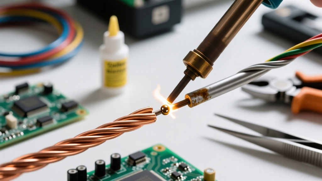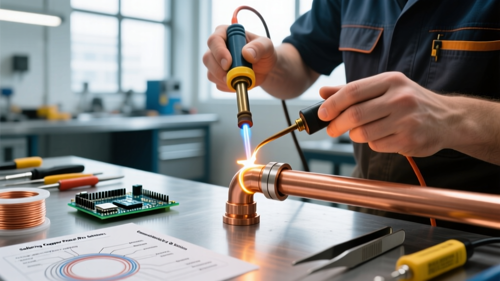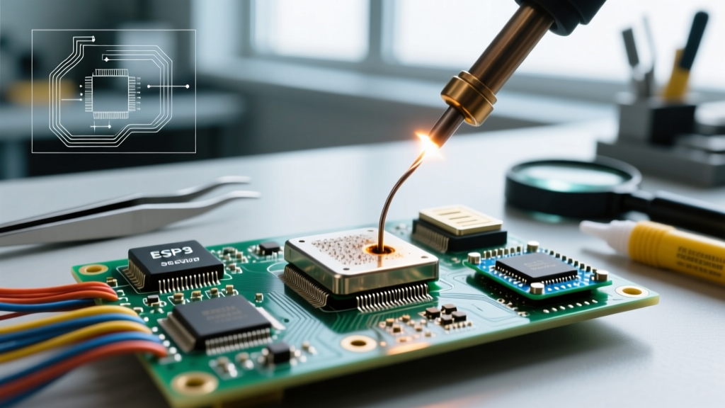

The Anatomy of a Cold Soldering Joint
A cold soldering joint occurs when the solder alloy fails to reach its liquidus temperature or lacks sufficient thermal energy to properly wet the copper pad and component lead. Instead of forming a reliable intermetallic compound (IMC) layer, the solder cools in a semi-molten or disturbed state. According to the IPC-A-610 standard for electronic assemblies, cold joints are classified as critical defects because they introduce high electrical resistance and are highly susceptible to mechanical fracturing under thermal cycling or vibration.
In modern 2026 electronics manufacturing and DIY repair, the transition to lead-free alloys like SAC305 (Sn96.5/Ag3.0/Cu0.5) has made cold joints more common. Lead-free solder requires higher temperatures and exhibits poorer wetting characteristics than traditional Sn63/Pb37 eutectic solder.
Visual and Physical Comparison
| Characteristic | Ideal Solder Joint | Cold Soldering Joint |
|---|---|---|
| Surface Appearance | Smooth, shiny, and reflective | Dull, grainy, lumpy, or frosty |
| Wetting Angle | Less than 90 degrees (concave fillet) | Greater than 90 degrees (convex beading) |
| Mechanical Strength | High (solid IMC layer formed) | Low (prone to micro-fractures) |
| Electrical Resistance | Negligible (milliohms) | Elevated (causes voltage drops and heat) |
5 Common Mistakes That Cause Cold Joints (And How to Fix Them)
Understanding the failure modes is the first step toward mastery. Here are the most frequent errors made by both hobbyists and professionals, along with precise solutions.
1. The Thermal Mass Trap (Incorrect Tip Selection)
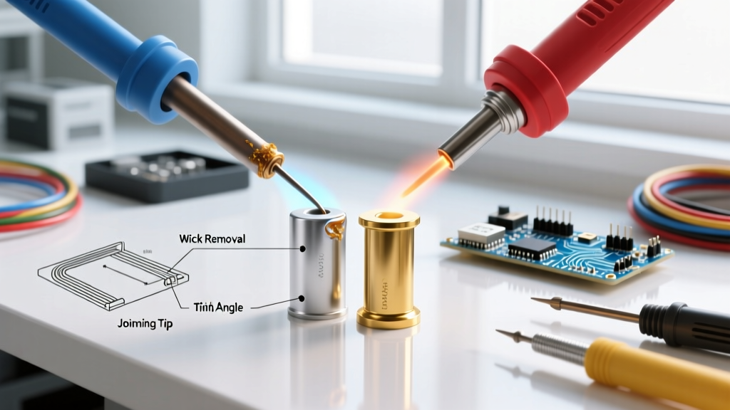
The Mistake: Using a fine 0.5mm conical tip (like the Hakko T18-B) to solder a large ground plane or a thick through-hole connector. The massive copper area acts as a heat sink, instantly draining thermal energy from the small iron tip. The solder melts on the iron but fails to transfer heat to the pad, resulting in a cold joint.
The Solution: Match the tip geometry to the thermal mass of the joint. For heavy ground planes, switch to a wide chisel tip (e.g., Hakko T18-D24 or Weller ETA) to maximize surface contact area. If using a station like the Hakko FX-888D (typically priced around $105-$115 in 2026), increase the dial to 360°C-380°C for SAC305 lead-free solder to compensate for the thermal drag.
2. The 'Disturbed Joint' Phenomenon
The Mistake: Moving the component or the PCB while the solder is in its critical plastic phase—the temperature window between the liquidus and solidus states. For SAC305, this occurs as the alloy cools from 217°C down to roughly 200°C. Movement during this 1-to-2-second window fractures the crystalline structure as it forms, creating a disturbed or cold joint that looks grainy and cracked.
The Solution: Implement a strict 'hands-off' rule. Use a PCB vise or a third-hand tool with silicone-tipped alligator clips to secure the board. After removing the iron, hold your breath and keep the board perfectly still for a full 3 seconds until the solder loses its liquid sheen.
3. Insufficient or Exhausted Flux Activation
The Mistake: Attempting to rework an oxidized pad without adding fresh flux. Flux is a chemical cleaning agent that removes copper oxide, allowing the molten solder to wet the metal. Without active flux, the solder balls up and refuses to flow, creating a cold, non-wetted joint.
The Solution: Always apply fresh flux before rework. For general through-hole and SMD work, use a no-clean rosin-based flux like Kester 245 FL-22 or Chip Quik SMD291AX. Apply a small amount with a precision syringe or brush, ensuring it covers both the pad and the lead before applying heat.
4. Applying Solder to the Iron, Not the Joint
The Mistake: Melting the solder wire directly onto the iron tip and attempting to 'carry' it to the joint like a bridge. By the time the molten solder touches the pad, its flux has boiled off and its temperature has dropped below the wetting threshold. This creates a cold, oxidized blob sitting on top of the pad rather than alloying with it.
The Solution: Follow the 'Heat-then-Feed' method. Touch the iron tip to the pad and lead simultaneously for 1 to 1.5 seconds. Then, feed the solder wire directly into the joint (opposite the iron tip). The joint's heat should melt the solder, not the iron.
5. Ignoring Tip Oxidation
The Mistake: Leaving a soldering iron on at 380°C for hours without tinning the tip. The iron plating oxidizes, forming a black, crusty layer that acts as a thermal insulator. Even if the station reads 380°C, the actual heat transfer to the joint is near zero.
The Solution: Never leave the iron bare. When pausing your work, apply a thick blob of SAC305 solder to the tip to shield it from oxygen. If oxidation has already occurred, use a brass wire sponge and a specialized tip tinner (like Hakko 599B) to chemically restore the wettable iron plating. Never use sandpaper or files, which will permanently destroy the tip's iron cladding.
Expert Insight: According to data published by the NASA Electronic Parts and Packaging (NEPP) Program, proper wetting requires the copper substrate to reach a minimum of 35°C above the solder's liquidus temperature. For lead-free SAC305 (liquidus 217°C), the pad itself must reach at least 252°C for a reliable intermetallic bond to form.
Step-by-Step Rework Procedure for Cold Joints
If you have identified a cold joint on your PCB, follow this precise rework protocol to restore reliability without lifting the delicate copper pad.
- Prep the Area: Clean the joint with 99% isopropyl alcohol (IPA) and a lint-free swab to remove old, carbonized flux residue.
- Apply Fresh Flux: Dispense a small drop of high-activity rosin flux over the cold joint.
- Select the Right Tool: If it is a large through-hole joint, use a desoldering pump or braided copper wick (e.g., Chemtronics 80-10-5) to remove the old, oxidized solder entirely.
- Re-tin and Heat: Set your station to 350°C. Apply a tiny amount of fresh solder to the tip to create a thermal bridge. Place the tip against the pad and lead simultaneously.
- Feed and Flow: Feed fresh solder wire into the joint until it flows smoothly into a concave fillet. Dwell time should not exceed 3 to 4 seconds to prevent delamination of the PCB substrate.
- Cool and Clean: Remove the iron and hold the board still. Once cooled, clean the residual flux with IPA to prevent long-term dendritic growth or corrosion.
Advanced Diagnostics: When Visual Inspection Fails
Sometimes, a cold soldering joint looks perfectly shiny but harbors internal micro-cracks or poor wetting beneath a surface layer of solder. In high-reliability applications, visual inspection is not enough.
Thermal Imaging (Joule Heating Test)
A cold joint suffers from elevated electrical resistance. When current flows through the circuit, the joint will dissipate power as heat (I²R losses). By powering the PCB and scanning it with a thermal camera (such as the FLIR C5 or a smartphone-attached FLIR One), you can identify hidden cold joints. A defective joint will appear as a localized 'hot spot' compared to adjacent healthy traces, often showing a temperature delta of 2°C to 5°C under normal operating loads.
Milliohm Continuity Testing
Standard multimeters lack the resolution to detect the minor resistance increase of a marginal cold joint. Use a specialized milliohm meter or a micro-ohmmeter to measure the voltage drop across the trace and component lead. A healthy joint should register less than 10 milliohms. Any reading fluctuating above 50 milliohms indicates a compromised intermetallic layer requiring immediate rework.
Conclusion
Eliminating the cold soldering joint from your workflow requires a shift from simply 'melting metal' to managing thermal dynamics and metallurgy. By respecting the thermal mass of your components, utilizing fresh flux, and adhering to strict dwell-time limits, you can achieve IPC-compliant, bulletproof connections every time. For further technical reading on soldering workmanship, consult the Hakko Technical Support library or the IPC-A-610 documentation to refine your bench skills.