
The Anatomy of a Flat Soldering Tip
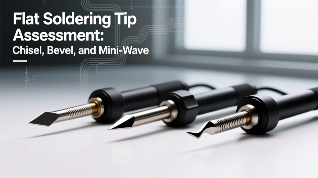
When building or repairing printed circuit boards (PCBs), the term flat soldering tip is frequently misunderstood as a single, monolithic tool shape. In reality, flat profiles encompass a spectrum of geometries, each engineered for specific thermal transfer requirements and joint formations. According to the NASA-STD-8739.3 Workmanship Manual, selecting the correct tip geometry is just as critical as temperature control; an improperly matched tip leads to cold joints, pad delamination, and excessive dwell times. In this tool-by-tool assessment, we dissect the three primary flat tip variants—Standard Chisel, Bevel (Hoof), and Mini-Wave—evaluating their real-world performance, thermal mass, and ideal use cases for 2026 electronics manufacturing and DIY rework.
Tool 1: The Standard Chisel (D-Tip)
Model Focus: Hakko T18-D24 & Weller RT4
The standard chisel, often designated as a "D-tip" by manufacturers like Hakko, features a flat, elongated face that tapers to a straight 90-degree edge. The Hakko T18-D24 (2.4mm width) and the Weller RT4 (0.062" width) are the undisputed workhorses of the modern electronics bench.
- Thermal Dynamics: The chisel tip concentrates thermal mass directly behind a narrow, flat edge. This allows for rapid heat penetration into plated through-holes (PTH) and heavy ground planes without requiring excessive station wattage.
- Optimal Applications: Point-to-point wiring, standard 2.54mm pitch through-hole components, and larger SMD passives (0805 and 1206 footprints). The flat edge allows the user to press flush against a component lead, maximizing surface contact.
- Pricing & Availability: Genuine Hakko T18-D24 tips retail between $8.50 and $11.00, while Weller RT4 tips sit around $12.50. Both are widely available and heavily cloned (though clones often suffer from premature iron plating dissolution).
Expert Insight: When working with lead-free SAC305 alloys, the chisel tip's narrow edge can oxidize rapidly if left idle. Always tin the flat face with a rosin-based (ROL0 or ROL1) flux-cored wire immediately after wiping to prevent de-wetting.
Tool 2: The Bevel / Hoof (C-Tip)
Model Focus: JBC C245-945 & Hakko T18-C3
The bevel tip, sometimes called a hoof tip, features a flat face that is cut at an angle (typically 45 to 60 degrees) and hollowed out to create a concave "belly." The JBC C245-945 (3.0mm bevel) and Hakko T18-C3 represent the pinnacle of this geometry.
- Thermal Dynamics: The concave belly acts as a solder reservoir. Unlike the chisel, which relies on manual solder feeding, the bevel tip holds a localized pool of molten solder via capillary action. This drastically reduces the thermal shock to sensitive SMD pads.
- Optimal Applications: Drag soldering SOIC, SOP, and TSOP integrated circuits. The belly holds just enough solder to bridge adjacent pins, while the angled point allows the user to drag across the IC legs, leaving clean, uniform fillets. It is also exceptional for scooping excess solder from tight busses.
- Pricing & Availability: JBC's C245 series commands a premium, typically $18.00 to $24.00 per tip, reflecting their integrated heater-sensor cartridge design which offers sub-second thermal recovery. Hakko's T18-C3 remains budget-friendly at roughly $9.00.
Tool 3: The Ultra-Flat Mini-Wave
Model Focus: Weller RTW2 & JBC C210-108
The mini-wave (or gull-wing) tip is a specialized, ultra-wide flat profile with a slight curvature at the very edge, mimicking the wave crest of an industrial selective soldering machine. The Weller RTW2 and JBC C210-108 are designed exclusively for high-density surface mount rework.
- Thermal Dynamics: These tips possess massive surface area but relatively low volumetric mass at the extreme edge. This design prevents the tip from bridging fine-pitch pads while providing a wide, even heat front.
- Optimal Applications: Drag soldering high-pin-count QFP (Quad Flat Package) and TQFP microcontrollers with 0.5mm or 0.4mm pitch. The mini-wave is the ultimate tool for clearing solder bridges on dense MCU footprints where a standard bevel tip would be too clumsy and a wick would lift the pads.
- Pricing & Availability: Due to the precision machining required to maintain flatness across a wide, thin edge, mini-wave tips are expensive. Expect to pay $22.00 to $35.00 per unit. They are also highly susceptible to mechanical damage if dropped.
Comparative Assessment Matrix
| Feature | Standard Chisel (D) | Bevel / Hoof (C) | Mini-Wave |
|---|---|---|---|
| Edge Geometry | Flat, 90° straight edge | Angled (45°-60°), concave belly | Wide, flat with micro-curve |
| Solder Capacity | Low (requires manual feed) | High (acts as reservoir) | Medium-High (surface tension) |
| Drag Soldering | Poor (causes bridging) | Excellent (SOIC/SOP) | Superior (QFP/TQFP) |
| Through-Hole | Excellent | Fair | Poor |
| Avg. Cost (2026) | $8 - $13 | $9 - $24 | $22 - $35 |
Thermal Dynamics and Alloy Matching
The effectiveness of any flat soldering tip is inextricably linked to the solder alloy in use. The IPC J-STD-001 Standard for Soldered Electrical and Electronic Assemblies outlines strict requirements for wetting and fillet formation, which are heavily influenced by tip temperature and alloy composition.
Leaded (63/37 SnPb) vs. Lead-Free (SAC305)
When using traditional 63/37 eutectic solder (melting point 183°C), a standard chisel tip set to 320°C provides ample thermal headroom for rapid wetting without degrading the flux core. However, modern SAC305 (Sn96.5/Ag3.0/Cu0.5) melts at 217°C and exhibits significantly poorer wetting characteristics. To achieve proper intermetallic compound (IMC) formation with SAC305 using a flat tip, operators must increase the station temperature to 350°C–380°C. This higher thermal demand accelerates iron plating dissolution on the flat face of the tip, a failure mode we will address next.
Failure Modes and Edge Cases
Even premium flat soldering tips from top-tier manufacturers will fail prematurely if subjected to improper maintenance. Understanding these failure modes is critical for maintaining a reliable workspace.
1. Iron Plating Dissolution and Pitting
The working surface of a soldering tip is a thin layer of iron plated over a copper core. When exposed to temperatures above 400°C—especially with aggressive, halide-activated lead-free fluxes—the iron layer dissolves into the molten solder. This exposes the underlying copper, which rapidly alloys with the tin, creating deep, black craters known as pitting. Once pitted, the flat surface loses its capillary action and will no longer hold solder.
2. Thermal Shock from Cellulose Sponges
Wiping a 380°C flat tip on a wet cellulose sponge causes an instantaneous temperature drop of up to 150°C. Over time, this thermal shock causes microscopic fractures in the iron plating. The NASA Workmanship Training Program heavily advocates for the use of dry brass wire wool for tip cleaning. Brass wool removes oxidized solder and carbonized flux without dropping the tip's thermal equilibrium, extending the life of flat profiles by up to 300%.
3. Mechanical Abrasion
Using a flat tip to scrape oxidized pads or pry up components will instantly gouge the iron plating. Flat tips, particularly the delicate edge of a mini-wave, should only be used for heat transfer and solder manipulation, never as a mechanical lever.
Final Verdict: Choosing Your Flat Profile
There is no universal "best" flat soldering tip; the correct choice is dictated entirely by your immediate task. Keep a 2.4mm Chisel on your primary station for general through-hole and wire tinning. Swap to a 3.0mm Bevel when drag soldering memory chips or logic gates. Finally, reserve the expensive Mini-Wave exclusively for high-pitch microcontroller rework and bridge removal. By matching the specific geometry to the joint requirement, you ensure IPC-compliant fillets, minimize thermal stress on your PCBs, and maximize the operational lifespan of your soldering accessories.