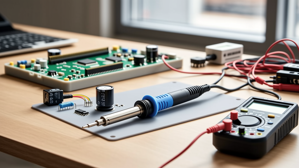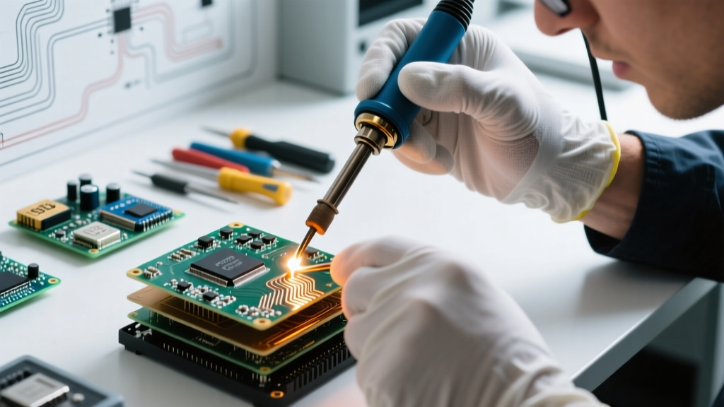

The Thermal Challenge of High-Layer-Count PCBs
As of 2026, the proliferation of 12-to-16-layer High-Density Interconnect (HDI) boards in consumer RF devices, automotive radar, and aerospace telemetry has fundamentally changed the rework landscape. When utilizing soldering irons on these complex assemblies, technicians face a severe thermodynamic hurdle: internal copper ground and power planes. These continuous copper pours act as massive heat sinks, rapidly drawing thermal energy away from the solder joint. If a technician relies on standard through-hole soldering techniques, the result is almost invariably a cold solder joint, pad delamination, or localized PCB warping.
Multi-layer PCBs require a nuanced understanding of thermal mass, active thermal recovery, and precise flux chemistry. According to the IPC-A-610 Acceptability of Electronic Assemblies standard, high-reliability (Class 3) solder joints demand specific wetting angles and fillet contours that are impossible to achieve if the thermal equilibrium of the joint is mismanaged. This guide details the exact methodologies required to master soldering irons for high-mass, multi-layer rework.
Matching Soldering Irons to PCB Complexity
Not all soldering irons are engineered to handle the thermal drain of a 10-layer board. The critical metric is not just peak wattage, but thermal recovery time—the speed at which the station's microcontroller detects a temperature drop at the tip and pushes current to the heating element. Below is a decision matrix for selecting the appropriate iron architecture based on PCB layer count and copper weight.
| PCB Layer Count | Copper Weight | Recommended Iron Architecture | Optimal Wattage & Tech | Example 2026 Station |
|---|---|---|---|---|
| 2 - 4 Layers | 1 oz (35 µm) | Standard Ceramic Heater | 40W - 60W (Passive) | Hakko FX-888D (~$110) |
| 6 - 8 Layers | 1 - 2 oz (Mixed) | Composite Sensor Heater | 60W - 80W (Active PID) | Hakko FX-951-2 (~$280) |
| 10 - 16 Layers | 2 oz+ (Heavy Ground) | Integrated Cartridge Tip | 130W+ (Direct RF/DC) | JBC CD-2BQF with C245 (~$460) |
For boards exceeding 8 layers with continuous internal ground planes, integrated cartridge systems (where the heater, sensor, and tip are a single unit) are mandatory. The physical distance between the sensor and the tip edge in cartridge systems is under 2 millimeters, allowing for sub-second thermal recovery when the tip contacts a massive ground plane via.
Tip Geometry and Alloy Metallurgy
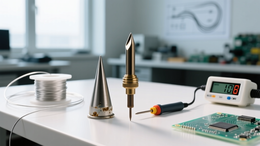
Selecting the correct tip geometry is just as critical as the station itself. A common mistake is using a fine conical tip (e.g., Hakko T12-I) for high-mass joints under the assumption that precision requires a small point of contact. In reality, a conical tip has minimal thermal mass and a tiny surface area, leading to instantaneous temperature collapse upon contact with a multi-layer PCB pad.
The Bevel and Chisel Advantage
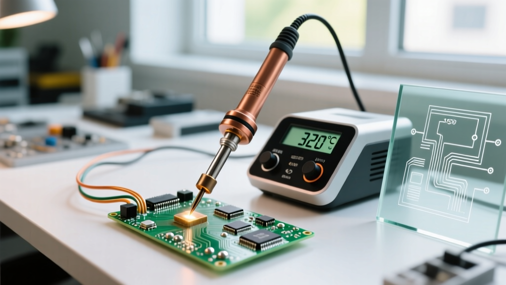
For multi-layer surface mount device (SMD) pads and large plated through-holes (PTH), a 45-degree bevel tip (like the JBC C245-945) or a wide chisel tip (Hakko T12-D24) is required. The flat surface area maximizes thermal transfer via conduction. When working with modern SAC305 (Sn96.5/Ag3.0/Cu0.5) lead-free alloys, which have a liquidus temperature of 217°C, the iron must be set between 360°C and 380°C. If you are still maintaining legacy Sn63/Pb37 (eutectic, 183°C liquidus) equipment, temperatures should be strictly regulated between 320°C and 340°C to prevent excessive flux burn-off.
Expert Insight: Never compensate for a lack of thermal mass by simply increasing the station temperature above 400°C. Excessive heat degrades the tip's iron plating, oxidizes the copper pad instantly (preventing wetting), and risks Z-axis delamination of the PCB substrate due to Coefficient of Thermal Expansion (CTE) mismatch.
Step-by-Step High-Mass Joint Technique
Executing a flawless solder joint on a 12-layer PCB requires a strict, repeatable sequence. This methodology ensures the pad, the component lead, and the solder wire reach the alloy's liquidus point simultaneously.
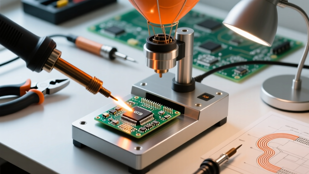
- Pre-Heat and Flux Application: Apply a high-activity, no-clean flux (such as Amtech NC-559-V2-TF, classified as ROL0) to the pad. For extremely dense ground planes, consider using a bottom-side PCB pre-heater set to 120°C to reduce the thermal delta the iron must overcome.
- Tip Tinning (The Thermal Bridge): Apply a microscopic amount of fresh solder to the tip of the iron immediately before contact. This creates a liquid metallic bridge that facilitates instantaneous heat transfer, bypassing the insulating effect of air gaps.
- Simultaneous Contact: Place the bevel or chisel tip so it bridges both the PCB pad and the component lead simultaneously. Hold for exactly 1.5 to 2.0 seconds to allow the flux to activate and clean the metallization.
- Feed the Solder: Introduce the solder wire (0.5mm to 0.8mm diameter) to the joint, not the tip. If the joint is at the correct temperature, capillary action will draw the molten alloy through the PTH barrel or under the SMD lead.
- Dwell and Withdraw: Allow the solder to flow and form a concave fillet (per IPC-A-610 Class 3 requirements). Total dwell time from initial iron contact to withdrawal must not exceed 3.5 seconds. Withdraw the solder wire first, then smoothly sweep the iron away at a 45-degree angle to prevent icicle formation.
Edge Cases and Failure Mode Analysis
Even with premium soldering irons, multi-layer rework presents unique failure modes. Recognizing these edge cases is the hallmark of a senior technician.
- Pad Cratering: This occurs when mechanical force is applied to the component while the solder is in its 'plastic' (semi-solid) state during the cooling phase. On multi-layer boards, the rapid heat dissipation can cause the solder to transition through the plastic phase unevenly. Solution: Use a third-hand tool or vacuum pickup to hold the component perfectly still until the joint turns completely dull and solid.
- Barrel Voiding in PTH: When soldering heavy ground pins, the solder may freeze at the top of the barrel before filling the via, leaving internal voids that fail X-ray inspection. Solution: Increase the iron's thermal mass (use a larger chisel tip) rather than the temperature, and apply flux directly into the barrel prior to heating.
- Tombstoning on SMDs: If one pad of a 0603 capacitor is connected to a massive internal plane and the other to a thin signal trace, the iron will heat the signal pad faster. The solder on the signal pad melts first, and surface tension pulls the component upright. Solution: Apply the iron's tip primarily to the ground-plane pad to equalize the thermal mass before introducing solder.
Metallurgical Maintenance Protocols
The lifespan of a soldering iron tip on multi-layer rework duty is directly tied to maintenance. Modern lead-free alloys like SAC305 are highly aggressive and will rapidly leach the iron plating from the tip if left untinned. According to Hakko's official tip care guidelines, oxidation accelerates exponentially above 350°C. Never leave a high-wattage station idle at operating temperature. Utilize the station's auto-sleep feature to drop the temperature to 150°C when the iron is holstered.
Furthermore, avoid using abrasive brass wool or damp sponges for cleaning during high-mass rework. A damp sponge causes thermal shock, which can micro-fracture the internal ceramic heater or the tip's iron plating. Instead, use high-temperature silicone tip cleaners or dry brass wire meshes, and always conclude your rework session by applying a thick layer of 63/37 leaded solder to the tip. This sacrificial layer protects the active iron plating from atmospheric oxidation until the next use.
For a broader understanding of foundational techniques that apply to both simple and complex assemblies, technicians should review the comprehensive soldering techniques guide on Electronics Notes. Mastering the intersection of tool selection, metallurgy, and thermodynamics is what separates adequate soldering from aerospace-grade reliability.