
Beyond the Basics: What's a Soldering Iron Really?
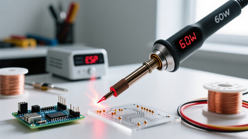
At its most fundamental level, a soldering iron is a localized thermal transfer tool designed to deliver precise, controlled heat to a specific junction. However, asking "what's a soldering iron" in a professional electronics context requires looking past the simple definition of a heated metal wand. It is an instrument of applied thermodynamics and metallurgy. The tool's primary job is not to melt solder directly; rather, its job is to elevate the thermal mass of the workpiece (the component lead and the PCB pad) above the solder's liquidus temperature so that capillary action and flux chemistry can create a permanent metallurgical bond.
In 2026, the market is divided between traditional resistive heating stations and advanced active-tip systems. While a basic 60W resistive iron might cost around $45, modern prosumer stations with active thermocouple feedback (like the Hakko FX-888D or Weller WE1010NA) range from $110 to $160. High-end active-tip systems, such as the JBC CD-2BQE, command upwards of $450, offering thermal recovery times measured in milliseconds rather than seconds.
The Internal Anatomy of a Modern Soldering Tip
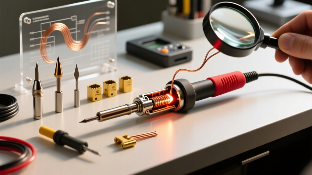
To master soldering techniques, you must understand the engineering of the tip itself. A high-quality replacement tip (such as the Hakko T18 series or Weller RT series) is a marvel of layered metallurgy designed to balance thermal conductivity with chemical resistance.
- Copper Core: The interior is solid copper, chosen for its exceptional thermal conductivity (approx. 401 W/m·K), rapidly pulling heat from the ceramic or nichrome heating element to the working surface.
- Iron Plating: Because molten solder aggressively dissolves bare copper (a process called leaching), the copper is electroplated with a layer of iron, typically 0.1mm to 0.5mm thick. This sacrifices a small amount of thermal conductivity for massive gains in tip lifespan.
- Chromium Barrier: A microscopic layer of chromium sits behind the iron plating to prevent solder from wicking up the shaft of the tip.
- Tinned Working Surface: Only the very end of the tip is pre-tinned with solder to ensure immediate thermal coupling with the workpiece.
Wattage vs. Thermal Recovery: The Ground Plane Problem
A common misconception is that higher wattage equals higher temperature. In reality, wattage dictates thermal recovery rate—how quickly the iron can replenish heat lost to the workpiece. When soldering a simple 0805 surface-mount resistor, a 40W iron is perfectly adequate. However, when soldering a heavy-gauge wire to a multi-layer PCB with internal copper ground planes, those planes act as massive heat sinks. A low-wattage iron will suffer from thermal droop, resulting in a cold joint.
| Application Type | Recommended Wattage | Thermal Mass Challenge | Ideal Tip Geometry |
|---|---|---|---|
| Micro SMD (0402 / 0603) | 20W - 40W | Low (tiny pads, minimal heat sinking) | Micro Conical / Fine Blade |
| Standard Through-Hole (ICs, Resistors) | 40W - 60W | Medium (standard FR4 pads and leads) | Standard Chisel (1.6mm - 2.4mm) |
| Heavy Ground Planes / RF Shields | 80W - 120W+ | High (copper pours rapidly drain heat) | Wide Chisel / Bevel (3.2mm+) |
| Plumbing / 10 AWG+ Wire | 150W - 300W | Extreme (massive copper volume) | Heavy Blowtorch / Massive Chisel |
The Metallurgy of the Joint: IMC and Wetting
When molten solder (such as eutectic Sn63Pb37 at 183°C or lead-free SAC305 at 217°C) contacts hot copper, a chemical reaction occurs, forming an Intermetallic Compound (IMC) layer, typically Cu6Sn5. According to research highlighted by the NASA Electronic Parts and Packaging (NEPP) Program, a reliable solder joint requires a thin, uniform IMC layer. If the iron is applied for too long or at excessive temperatures, the IMC layer grows too thick, becoming brittle and prone to mechanical fracturing under vibration or thermal cycling.
Expert Insight: The goal of flux is to dissolve metal oxides on the pad and lead, allowing the molten solder to 'wet' the bare metal. If your solder balls up and rolls off the pad like water on a waxed car, you have a wetting failure caused by oxidation, not a temperature failure.
Core Technique: The 4-Step Through-Hole Method
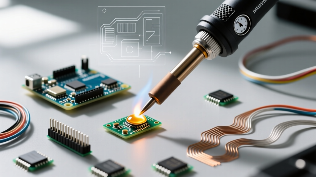
Mastering what's a soldering iron used for requires strict adherence to thermal discipline. As detailed in the foundational SparkFun Through-Hole Soldering Tutorial, the iron should always heat the workpiece, not the solder directly.
- Clean and Tin the Tip: Wipe the tip on a damp brass sponge (never use excessive water, which causes thermal shock and micro-fractures in the iron plating). Apply a tiny amount of fresh solder to the tip to create a thermal bridge.
- Simultaneous Contact: Place the flat face of the chisel tip so it touches both the copper pad and the component lead simultaneously. Hold for 1 to 2 seconds.
- Feed the Solder: Touch the solder wire to the opposite side of the joint (where the pad and lead meet), not directly to the iron tip. If the workpiece is hot enough, the solder will instantly melt and wick into the barrel via capillary action.
- Withdrawal Sequence: Remove the solder wire first, then smoothly pull the iron away at a 45-degree angle. This prevents 'solder icicles' and leaves a clean, concave fillet.
Tip Selection Matrix for Precision Work
Using the wrong tip geometry is the leading cause of damaged PCB pads and lifted traces. The Adafruit Guide to Excellent Soldering emphasizes matching the tip's thermal mass to the joint's physical size.
| Tip Shape | Best Use Case | Failure Mode if Misused |
|---|---|---|
| Conical (Point) | Touch-up, micro-SMD, tight spaces. | Poor thermal transfer on large pads; point oxidizes rapidly. |
| Chisel (Flat) | General through-hole, SMD drag soldering. | Can bridge tight-pitch IC pins if too wide. |
| Bevel (Hoof) | Drag soldering SMT ICs, holding large blobs of solder. | Poor precision for discrete, isolated components. |
| Knife (K-Tip) | Corner cleaning, cutting through solder bridges, SMD rework. | Can easily slice into FR4 substrate if pressed too hard. |
Troubleshooting Edge Cases and Failure Modes
Even with a high-end station, improper technique yields defective joints. Understanding these failure modes is critical for rework and quality control.
1. The Disturbed Joint (Grainy Appearance)
If the component moves while the solder is transitioning from a liquid to a solid state (the plastic phase), the IMC crystallization is disrupted. The resulting joint looks grainy, dull, and frosty. Fix: Apply flux and reflow the joint with a clean iron, holding the component perfectly still until the solder fully solidifies.
2. Pad Lifting and Delamination
FR4 PCB substrates utilize epoxy resins with a Glass Transition Temperature (Tg) typically between 130°C and 170°C. If you apply a 400°C iron to a pad for more than 5-7 seconds, the localized epoxy softens, and the mechanical stress of the iron can peel the copper pad entirely off the board. Fix: Use a higher wattage iron with a larger tip to reduce the time required to reach soldering temperature, rather than turning up the temperature dial.
3. Tip Oxidation (The 'Black Crust')
Leaving a station idle at 350°C without a protective blob of solder causes the iron plating to oxidize, turning black and refusing to accept new solder. Fix: Never file or sand an oxidized tip; this destroys the iron plating and ruins the tool. Instead, use a specialized tip tinner/activator paste (like Hakko 599B) or aggressively rub it in a brass wire sponge while applying fresh, heavily fluxed 63/37 solder.
Final Thoughts on Tool Selection
Understanding what's a soldering iron means recognizing it as a precision thermal management system. Whether you are building a simple Arduino sensor array or reworking a dense BGA chipset, success relies on matching the tool's thermal recovery capabilities to the joint's mass, selecting the correct metallurgical alloy, and respecting the chemical limits of your flux. Invest in a station with closed-loop temperature sensing, maintain your tips rigorously, and let thermodynamics do the heavy lifting.