
The Thermal Reality of Surface Mount Assembly
Transitioning from traditional through-hole soldering to surface mount technology (SMT) requires a fundamental shift in how you approach thermal management. When setting up a soldering iron for surface mount components, the primary challenge is the drastic reduction in thermal mass. A standard TO-220 transistor can absorb significant heat before its internal junction is compromised, but a delicate 0402 metric ceramic capacitor or a fine-pitch QFP (Quad Flat Package) IC will suffer catastrophic failure, pad delamination, or internal cracking if subjected to uncalibrated thermal spikes.
As of 2026, the industry standard has pushed heavily into 0201 and even 01005 metric components. At these microscopic scales, the margin for error in temperature control is virtually zero. According to IPC assembly standards, the ideal intermetallic compound (IMC) layer between the component lead and the copper pad should be between 1 and 3 microns thick. If your soldering station is improperly calibrated and runs too hot, the IMC layer grows excessively thick, resulting in a brittle solder joint that will fail under mechanical or thermal stress. Conversely, an under-calibrated iron leads to cold joints, poor wetting, and the dreaded 'tombstoning' effect.
Essential Calibration Equipment for SMD Work
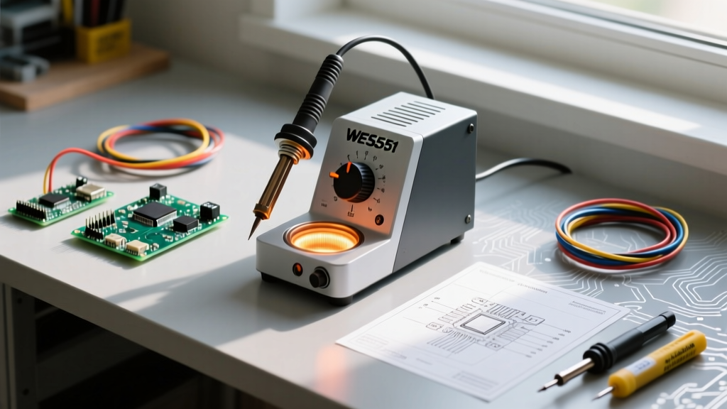
You cannot calibrate a high-precision SMD station by guessing or relying solely on the digital readout of the base unit. The digital display shows the temperature of the heating element or the internal sensor, not the actual temperature at the very tip of the iron where the solder wetting occurs. To properly set up your workstation, you need the following tools:
- Tip Thermometer: The Hakko FG-100B (approximately $240) or a high-quality dual-channel K-type thermocouple meter like the Fluke 52 II ($350). These devices measure the actual surface temperature of the tip with a response time of under 2 seconds.
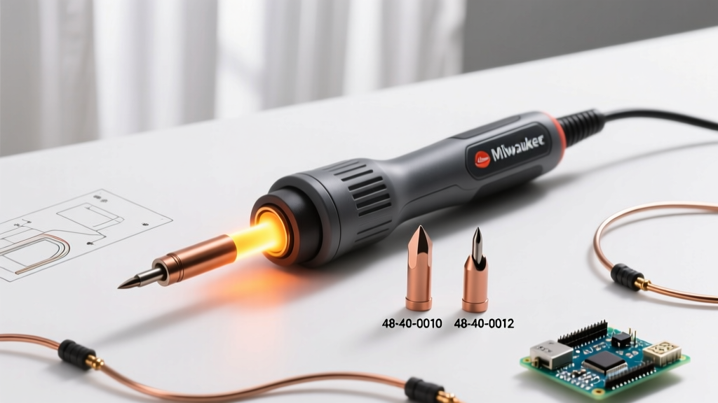
- SMD-Specific Soldering Tips: For active-tip systems like the JBC CD-2BQE, the C115 series (e.g., C115-112 blade or C115-108 conical) is mandatory for 0402 work. For passive cartridge systems like the Hakko FX-951, the T12-IL or T12-K (knife) tips offer the best thermal transfer for SMD.
- Thermal Test Board: A dummy FR4 board with copper ground planes and thermal vias to test thermal recovery under load.
- High-Activity Flux: A no-clean tacky flux (e.g., Amtech NC-559-V2-TF) to assist in heat transfer during the calibration wetting tests.
Step-by-Step SMD Soldering Iron Calibration Protocol
Follow this exact procedure to map and adjust your station's thermal offset, ensuring the tip temperature perfectly matches your target SMD profile.
Step 1: Establish the Baseline Target
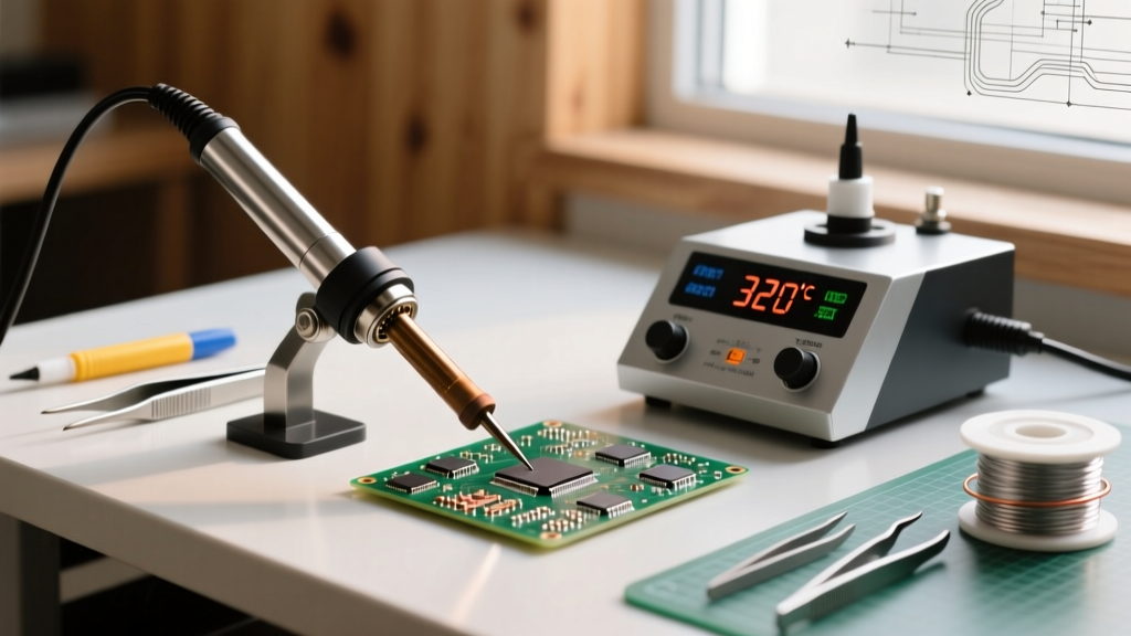
For standard lead-free SAC305 (Sn96.5/Ag3.0/Cu0.5) solder paste and wire, the liquidus temperature is 217°C. However, the tip must be hotter to transfer heat rapidly. Set your station's target temperature to 340°C (644°F). This provides a 123°C delta, which is sufficient to melt the solder and achieve proper wetting within 1.5 to 2.0 seconds without scorching the FR4 substrate.
Step 2: Measure the Static Offset
Apply a tiny dab of fresh solder to the very end of your SMD tip to create a thermal bridge. Press the thermocouple sensor of your Hakko FG-100B directly into the molten solder bead on the tip. Wait for the reading to stabilize (usually 5 to 8 seconds). If your station reads 340°C but the thermometer reads 325°C, you have a -15°C static offset. Use your station's calibration menu to input this offset value.
Step 3: Dynamic Thermal Recovery Testing
Static calibration is only half the battle. SMD components are often placed near ground planes or thermal vias that act as heat sinks. Touch your newly calibrated tip to a large copper pour on your test board and apply a 0.5mm diameter strand of SAC305 solder. Use a thermal camera or an embedded thermocouple to monitor how fast the temperature drops and recovers. A properly calibrated JBC active-tip station should recover to 340°C in under 1.2 seconds. A standard Hakko T12 cartridge may take 2.5 to 3.5 seconds.
Expert Insight: Never calibrate an SMD tip using a dry tip. The oxidation layer on a dry tip acts as a thermal insulator, leading to false-low readings on your thermocouple. Always use a small solder bridge or high-activity flux to ensure accurate thermal coupling between the tip and the sensor.
Calibration Data Matrix: Top SMD Stations Compared
Different heating architectures handle SMD thermal loads differently. Below is a comparison of how three popular 2026 market leaders perform when calibrated for 0402 and fine-pitch IC work.
| Station Model | Heating Architecture | Target Temp | Measured Static Offset | Thermal Recovery (Ground Plane) | Approx. Cost |
|---|---|---|---|---|---|
| JBC CD-2BQE (C115 Tip) | Active (Heater in tip) | 340°C | +/- 2°C | < 1.0 Second | $650 |
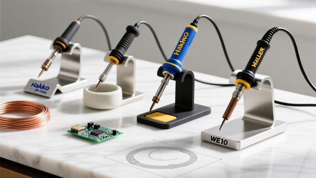
| Hakko FX-951 (T12-IL) | Passive Cartridge | 340°C | +/- 8°C | 2.5 - 3.5 Seconds | $320 |
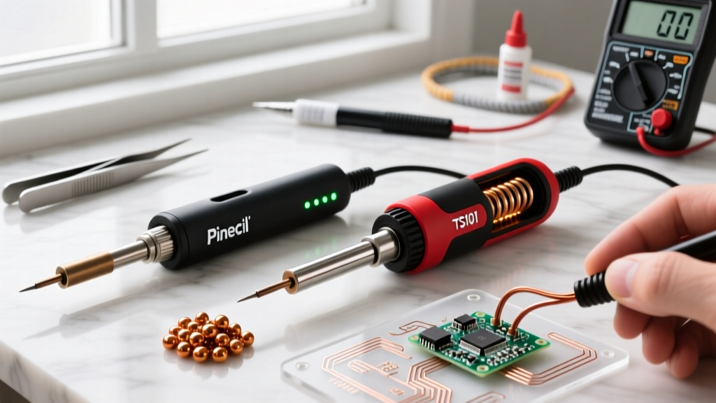
| Pinecil V2 (TS-B2 Tip) | Direct DC Cartridge | 340°C | +/- 12°C | 4.0 - 5.0 Seconds | $26 |
| Weller WX2021 (RTW3) | Active (Heater in tip) | 340°C | +/- 3°C | < 1.2 Seconds | $780 |
As the data illustrates, active-tip systems from JBC Tools and Weller offer vastly superior thermal recovery, which is critical when dragging a knife tip across a 100-pin QFP chip where the ground pins are connected to massive internal copper planes.
Optimizing Tip Geometry for Calibrated Heat Transfer
Calibration is useless if the physical geometry of the tip cannot transfer the calibrated heat into the joint. For SMD work, the contact area dictates the thermal transfer rate.
- Conical Tips (e.g., C115-108): Excellent for 0201 and 0402 discrete components. The tiny surface area prevents accidental bridging but requires flawless calibration because the thermal mass of the tip itself is incredibly low.
- Knife / Blade Tips (e.g., T12-K, C115-112): The ultimate SMD workhorse. By using the edge of the knife for 0402s and the flat side for dragging solder across SOIC or QFP pins, you maximize thermal transfer without increasing the station temperature.
- Mini-Hoof / Gull-Wing Tips: Ideal for rework and removing SMD ICs. The concave shape holds a small reservoir of molten solder, which acts as a thermal bridge to heat all pins of an IC simultaneously.
Flux Chemistry and Thermal Calibration Interaction
A frequently overlooked aspect of setting up a soldering iron for surface mount components is the interaction between your calibrated tip temperature and the flux activation window. Most high-quality no-clean fluxes (like Indium NC-213 or Kester 233) have an activation temperature ranging from 150°C to 180°C.
If your iron is calibrated too low (e.g., 280°C), the flux may activate, but it will burn off before the solder reaches its 217°C liquidus state, leaving you with oxidized, unmelted solder balls. If calibrated too high (e.g., 390°C), the flux splatters and boils violently, causing microscopic solder spheres to lodge under BGA components or fine-pitch leads, creating hidden short circuits. Maintaining a strict 340°C to 350°C calibration ensures the flux remains active just long enough to reduce the copper oxides and allow the molten solder to flow via capillary action.
Troubleshooting Common SMD Calibration Failures
Even with a calibrated station, specific edge cases can mimic poor calibration. Here is how to diagnose and fix them:
1. Pad Lifting and Delamination
Symptom: The copper pad detaches from the FR4 substrate when removing the iron.
Diagnosis: This is rarely a temperature issue; it is a dwell-time issue. The glass transition temperature (Tg) of standard FR4 is around 130°C to 150°C. If you hold a 340°C iron on a pad for more than 3 seconds, the localized heat penetrates the board, softening the epoxy resin. Fix: Apply more flux to lower the surface tension and speed up wetting, reducing dwell time to under 1.5 seconds.
2. Tombstoning on 0402 Components
Symptom: One side of the capacitor solders, but the other side stands straight up.
Diagnosis: Uneven thermal transfer. One pad is connected to a ground plane via a thermal relief, while the other is connected to a thin trace. The ground plane absorbs the heat faster, causing the solder on the trace side to melt and pull the component upright via surface tension. Fix: Pre-heat the ground-plane pad for 0.5 seconds before applying solder to both pads simultaneously, or use a lower temperature profile (320°C) with a highly active liquid flux to equalize the wetting time.
3. Solder Wicking Up the Lead
Symptom: Solder climbs up the IC lead away from the PCB pad, leaving a starved joint.
Diagnosis: The iron tip is touching the component lead before it touches the PCB pad. Heat travels up the lead, melting the solder there first. Fix: Adjust your physical technique. Always touch the tip to the PCB pad and the very heel of the component lead simultaneously, ensuring the pad reaches the liquidus temperature first.
Final Verification and Maintenance
Calibration is not a one-time event. SMD tips, particularly the ultra-fine C115 and T12 variants, degrade rapidly due to the high flux activity and frequent cleaning required. The iron plating on the tip erodes, creating microscopic pitting that ruins thermal transfer. As a best practice in any professional 2026 SMD rework lab, verify your tip's static offset using a thermocouple meter at the start of every shift. If the offset drifts beyond +/- 10°C, or if you notice the solder taking longer than 2 seconds to wet, discard the tip immediately. Investing $55 in a fresh JBC C115 tip is vastly cheaper than scrapping a $500 populated PCB due to a compromised solder joint.