
The Thermodynamics of Proper Soldering Iron Use
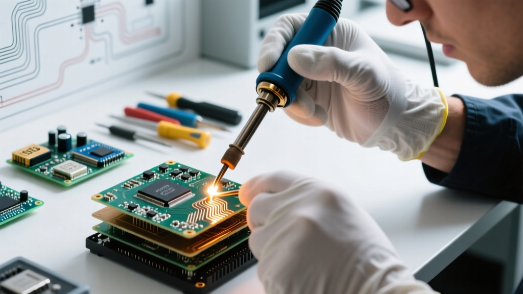
Learning how to use a soldering iron properly is less about melting metal and more about managing thermodynamics. Many hobbyists and junior technicians treat the iron as a glue gun, applying molten solder to the iron's tip and attempting to transfer it to the joint. This 'painting' method results in cold joints, flux burnout, and severe reliability failures. Expert soldering iron use requires understanding that the iron is a heat delivery system, not a solder delivery system. The goal is to raise the temperature of the component lead and the printed circuit board (PCB) pad simultaneously until they are hot enough to melt the solder wire upon contact.
According to the IPC-A-610 standard for electronic assemblies, a reliable through-hole or surface-mount joint requires proper wetting, characterized by a smooth, concave fillet with a wetting angle of less than 90 degrees. Achieving this requires precise control over temperature, tip geometry, and flux chemistry.
Calibrating Your Station: Temperature Profiles for Modern Alloys
In 2026, the transition to lead-free alloys is absolute in commercial manufacturing, though Sn63/Pb37 (leaded) remains popular in hobbyist and aerospace prototyping circles due to its lower melting point and superior fatigue resistance. Your station's temperature dial must be matched to the alloy's melting point plus the thermal mass of the joint.
| Alloy Designation | Composition | Melting Point | Recommended Iron Temp | Max Dwell Time |
|---|---|---|---|---|
| Sn63/Pb37 (Eutectic) | 63% Tin, 37% Lead | 183°C (361°F) | 315°C - 330°C | 1.5 - 2.5 seconds |
| SAC305 (Lead-Free) | 96.5% Sn, 3% Ag, 0.5% Cu | 217°C (422°F) | 350°C - 380°C | 2.0 - 3.5 seconds |
| Sn99.3/Cu0.7 | 99.3% Tin, 0.7% Copper | 227°C (440°F) | 360°C - 390°C | 2.5 - 4.0 seconds |
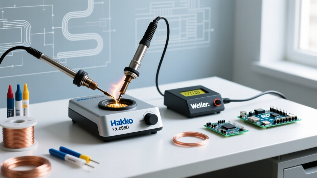
Expert Insight: Never exceed 400°C (752°F) on a standard PCB. FR-4 fiberglass substrates typically have a Glass Transition Temperature (Tg) between 130°C and 170°C. Prolonged exposure to extreme iron temperatures will cause delamination, pad lifting, and via barrel cracking. A high-quality station with rapid thermal recovery, such as the Hakko FX-888D ($115–$130) or the Weller WE1010NA ($120), allows you to run lower temperatures while maintaining sufficient heat transfer, protecting both your board and your tips.
Tip Geometry: Matching the Tool to the Pad
The most common mistake in soldering iron use is defaulting to a fine conical tip (like the Hakko T18-B) for all tasks. Conical tips have a microscopic surface area at the point of contact, resulting in terrible thermal transfer. They are only suitable for ultra-fine pitch SMD work (0.4mm pitch or smaller).
- Chisel Tips (e.g., Hakko T18-D24, Weller ETA): The workhorses of the bench. The flat, 30-degree beveled face maximizes surface area contact with both the pad and the lead simultaneously. A 2.4mm chisel is ideal for standard 0.1-inch through-hole components and 0805/0603 SMD pads.
- Bevel/Hoof Tips (e.g., Hakko T18-C2): Excellent for drag-soldering SOIC and QFP surface-mount ICs. The concave 'hoof' holds a small reservoir of molten solder, allowing surface tension to pull the solder evenly across the pins.
- Knife Tips (e.g., Weller Weller K): Perfect for cutting through solder bridges on fine-pitch components and cleaning up pad arrays on BGA footprints.
The Golden Rule of Tip Selection: Always choose the largest tip geometry that will physically fit on the pad without bridging to adjacent copper. Maximum mass equals maximum thermal transfer, allowing you to complete the joint faster and at a lower temperature.
The 4-Step IPC Execution Protocol
To achieve Class 2 or Class 3 reliability standards as outlined by NASA's Electronic Parts and Packaging (NEPP) program, follow this strict four-step sequence for every single joint.
- Clean and Tin the Tip: Wipe the tip on a dry brass wool sponge (never a wet cellulose sponge, as the rapid thermal shock causes micro-cracking in the tip's iron plating). Apply a microscopic amount of solder to the tip to create a 'thermal bridge'.
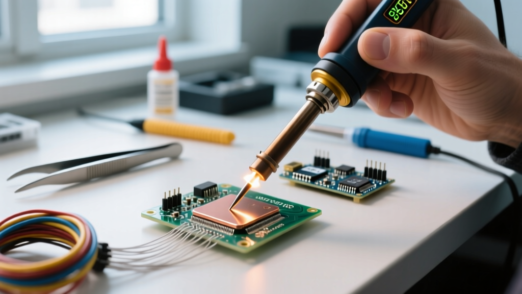
- Heat the Joint: Place the flat face of the chisel tip so it touches both the component lead and the PCB pad simultaneously. Hold for 1 to 2 seconds. You are heating the metal, not the air.
- Feed the Solder: Introduce the solder wire to the opposite side of the joint, not directly to the iron tip. If the joint is hot enough, the solder will flash-melt and wick into the via or around the lead via capillary action. Feed exactly enough to form a concave fillet.
- Withdraw and Cool: Remove the solder wire first, then sweep the iron away at a 45-degree angle. Allow the joint to cool naturally for 2-3 seconds. Do not blow on the joint. Forcing a rapid cool creates a 'disturbed joint,' characterized by a dull, grainy crystalline structure that is highly prone to mechanical failure.
Flux Chemistry: The Unsung Hero of Wetting
You cannot master how to use a soldering iron without mastering flux. Flux is a chemical reducing agent that strips metal oxides from the copper pad and component lead at high temperatures, allowing the molten solder to metallurgically bond (intermetallic layer formation) rather than just sitting on top like water on a waxed car.
For manual bench work, rely on external liquid or gel fluxes rather than trusting the rosin core inside your solder wire alone. Kester 186 RMA (Rosin Mildly Activated) remains the gold standard for leaded aerospace and prototyping work, requiring an isopropyl alcohol (IPA) cleanup post-soldering. For modern lead-free SMD rework, no-clean synthetic fluxes like Amtech NC-559-V2-TF leave a benign, high-resistivity residue that does not require washing, saving time and preventing moisture intrusion from cleaning solvents.
Troubleshooting Common Failure Modes
Even with premium equipment like a JBC CD-2BQF or a Metcal PS-900, improper technique will yield defective joints. Here is how to identify and correct the most common errors:
1. The Cold Joint
Symptom: The solder forms a convex, lumpy ball that sits on the pad rather than flowing into it. The surface is dull and gray.
Cause: Insufficient heat applied to the pad/lead, or attempting to transfer solder from the iron tip to the joint.
Correction: Increase station temperature by 15°C. Apply fresh liquid flux. Reheat the joint directly with the iron until the existing solder reflows and wicks properly.
2. Solder Icicles and Webbing
Symptom: Sharp spikes of solder hanging from the joint, or thin webs bridging adjacent pins.
Cause: Excessive solder feed, insufficient flux, or withdrawing the iron too slowly.
Correction: Apply a generous amount of gel flux to the area. Use a clean, tinned chisel tip to reheat the joint; the flux's surface tension activators will pull the excess solder back onto the tip and smooth the fillet.
3. Pad Lifting and Delamination
Symptom: The copper pad separates from the fiberglass substrate, sometimes tearing the trace entirely.
Cause: Dwell time exceeded 4 seconds, or iron temperature set above 420°C on standard FR-4.
Correction: Use a larger chisel tip to transfer heat faster, reducing the required dwell time. If repairing a lifted pad, scrape the trace, bond the pad back down with cyanoacrylate (CA) glue, and install a 30 AWG copper jumper wire to restore the circuit.
Mastering soldering iron use is a continuous practice of thermal management and chemical preparation. By respecting the metallurgy of your alloys and adhering to strict IPC execution protocols, you will produce joints that are not only visually flawless but engineered to survive decades of thermal cycling and mechanical vibration.
Further Reading and Industry Standards
To deepen your understanding of solder metallurgy and reliability testing, consult the Indium Corporation's Engineering Blog for extensive whitepapers on SAC305 fatigue resistance and the effects of bismuth doping in low-temperature alloys. Always benchmark your manual workmanship against the visual acceptance criteria defined in your industry's specific regulatory framework.