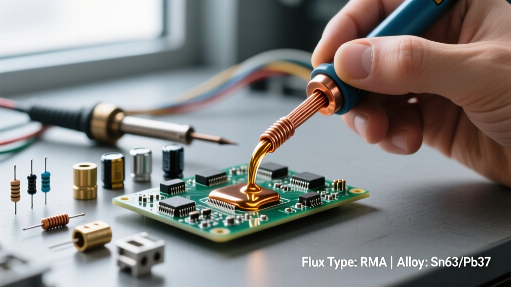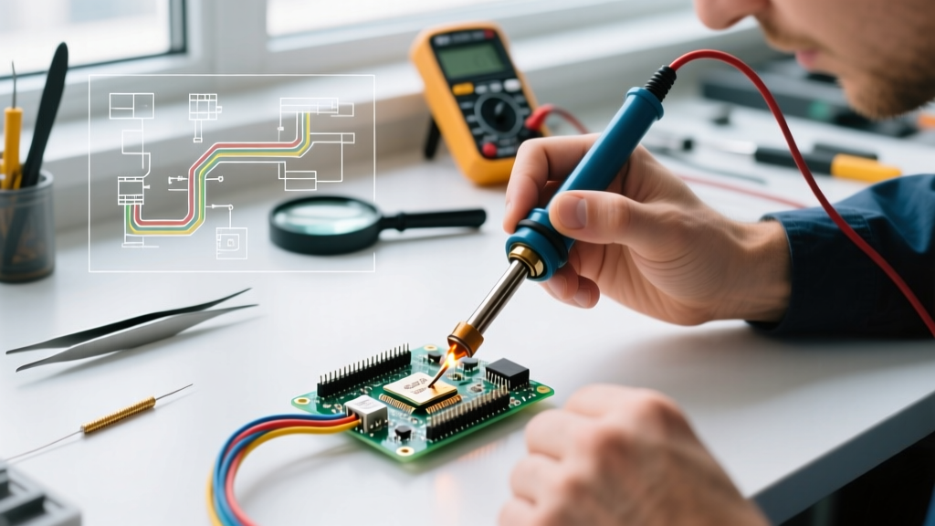

Mastering the Soldering Training Certification Exam
Earning an IPC certification is a career-defining milestone for electronics manufacturing professionals. However, the practical exams for a soldering training certification are notoriously rigorous. Instructors evaluate your work against strict, unforgiving criteria, and even minor deviations in thermal management or wetting angles can result in an immediate fail. Whether you are pursuing the IPC J-STD-001 (Requirements for Soldered Electrical and Electronic Assemblies) or the IPC-A-610 (Acceptability of Electronic Assemblies), understanding why candidates fail is the first step toward passing.
This guide serves as a comprehensive troubleshooting manual and FAQ for technicians preparing for their 2026 certification exams. We will dissect the most common practical test failures, provide actionable corrections, and outline the exact parameters you need to master to secure your Certified IPC Specialist (CIS) credentials.
The Core Standards: What Examiners Are Looking For
Before troubleshooting specific defects, you must understand the framework examiners use to grade your work. The IPC standards do not just look for 'good' or 'bad' solder joints; they categorize conditions into three distinct classes:
- Target Condition: The ideal, perfect joint. While not always required to pass, it represents optimal reliability.
- Acceptable Condition: The joint may not be perfect, but it meets the minimum requirements for reliability and will pass the exam.
- Defect Condition: The joint fails to meet minimum criteria and will result in a failing grade for that specific module.
According to the IPC J-STD-001 Standard, examiners are trained to look for specific metallurgical and mechanical characteristics. You must demonstrate consistent control over your soldering iron temperature, flux application, and wetting time.
Troubleshooting the Top 5 Certification Test Failures
Based on data from leading training centers, over 70% of practical exam failures stem from five specific soldering defects. Here is how to identify, troubleshoot, and correct them before your test day.
1. Disturbed Solder Joints (Cold or Frosty Solder)
The Failure: The solder joint exhibits a dull, gray, or frosty appearance with visible graininess. In severe cases, the joint may show a physical separation line or 'disturbed' crystalline structure.
The Cause: Movement of the component or wire while the solder is transitioning from a liquid to a solid state (the plastic phase). It can also be caused by insufficient heat, preventing the flux from fully activating and the solder from properly alloying with the base metals.
The Fix:
- Ensure your workstation is ergonomically set up so your hands are fully supported. Use a PCB holder or third-hand tool to eliminate board movement.
- Verify your iron temperature. For SAC305 lead-free solder, set your station (e.g., JBC CD-2BQE or Hakko FX-951) to 340°C - 350°C. If using Sn63/Pb37, 315°C is usually sufficient.
- Apply heat to the pad and lead simultaneously for 1-2 seconds before introducing the solder wire. Remove the solder wire first, then the iron, and hold the component perfectly still for 3-4 seconds until the joint solidifies.
2. Insufficient Wetting and Non-Wetting
The Failure: The solder balls up on the pad or lead rather than flowing out and forming a smooth, concave fillet. The contact angle exceeds 90 degrees (non-wetting) or fails to form a continuous, smooth transition (insufficient wetting).
The Cause: Oxidation on the component leads or PCB pads, expired or insufficient flux, or inadequate thermal transfer to the joint surfaces.
The Fix:
- Inspect the test components. If leads are oxidized, gently clean them with a fiberglass scratch pen or isopropyl alcohol (IPA) before soldering.
- Use a high-quality rosin-based flux (ROL0 or ROL1 classification). Apply a small amount of liquid or gel flux to the joint before heating.
- Tin your iron tip immediately before making contact with the joint. A tinned tip increases the surface area for thermal transfer, ensuring the pad reaches the solder's melting point faster.
3. Solder Bridging and Shorts
The Failure: Solder flows between two adjacent pads or pins, creating an electrical short. This is an automatic defect in all IPC classes.
The Cause: Using too much solder, using an iron tip that is too large for the pitch spacing, or dragging the iron across fine-pitch SMD components without proper flux.
The Fix:
- Match your tip geometry to the pad size. For 0.5mm pitch QFPs, use a micro-pencil or a specialized hoof tip no wider than 0.4mm.
- Rely on flux, not excessive solder. Apply generous amounts of no-clean flux and use the surface tension of the molten solder to pull it into the joints.
- If a bridge occurs during the exam, do not panic. Apply fresh flux, use a clean, tinned iron tip to 'lift' the excess solder away, or use high-quality copper desoldering braid (e.g., Chemtronics 80-5-5) to wick away the short.
4. Component and PCB Damage
The Failure: Scorched PCB laminates, lifted pads, melted connector housings, or heat-shrunk wire insulation pulled back more than the allowable limit.
The Cause: Dwell time exceeding the maximum allowable limit (typically 3 to 5 seconds per joint) or using an iron temperature that is too high for the thermal mass of the component.
The Fix:
- Practice the '3-second rule'. If the joint is not completed within 3 seconds, remove the iron, let the board cool for 10 seconds, and try again.
- For heat-sensitive components like electrolytic capacitors or plastic connectors, use a thermal shunt (like a hemostat clipped to the lead) to draw heat away from the component body.
- Keep your tip clean. A dirty, oxidized tip requires longer dwell times because carbon buildup acts as a thermal insulator. Clean your tip in a damp brass sponge every 3-4 joints.
5. Insufficient Solder Fill in Plated Through-Holes (PTH)
The Failure: The solder does not wick completely through the barrel of the plated through-hole.
The Cause: Insufficient heat applied to the barrel, or the solder was applied to the iron tip rather than the joint, causing the flux to burn off before it could pull the solder through the hole via capillary action.
The Fix:
- Always apply the iron to the lead and the inside wall of the barrel simultaneously.
- Feed the solder wire into the joint opposite the iron tip. The heat will draw the solder through the barrel.
- For Class 3 certification, you must achieve 100% fill and wetting on both sides of the board. Preheating the bottom side of the board with a hot air gun set to 120°C can drastically improve capillary flow for heavy ground-plane connections.
Comparison Matrix: IPC Class Requirements for PTH Joints
Understanding the exact fill requirements for Plated Through-Holes (PTH) is critical for your practical exam. The table below outlines the minimum acceptable fill percentages based on the NASA Workmanship Standards and IPC J-STD-001 guidelines, which are frequently used as benchmark references in advanced training.
| IPC Class | Product Type | Minimum PTH Fill (Solder Side) | Wetting Requirement |
|---|---|---|---|
| Class 1 | General Electronic Products | 50% | Wetting required on solder side |
| Class 2 | Dedicated Service Electronics | 75% | Wetting required on both sides |
| Class 3 | High-Performance / Life Support | 100% | 100% fill and wetting on both sides |
Soldering Training Certification FAQ
Navigating the administrative and logistical side of certification can be just as confusing as the technical requirements. Here are the most frequently asked questions from candidates in 2026.
How much does a soldering training certification cost?
As of 2026, the cost for an initial Certified IPC Specialist (CIS) course typically ranges from $1,200 to $1,800 USD for a 3-to-4-day class. This price generally includes the training manual, hands-on lab materials, and the certification exam fee. Advanced courses, such as the IPC 7711/7721 (Rework, Modification, and Repair), may cost up to $2,200 due to the specialized rework equipment and consumables required. You can find detailed pricing breakdowns through authorized providers like Blackfox IPC Certification Training.
How long is the certification valid, and how do I renew it?
IPC certifications are valid for exactly two years from the date of your initial passing grade. To maintain your credentials without retaking the full multi-day course, you must complete a recertification module within the 90 days prior to your expiration date. Recertification typically takes 1 to 2 days and costs between $600 and $900. If your certification lapses, you are required to retake the full initial CIS course.
What is the difference between CIS and CIT?
A CIS (Certified IPC Specialist) is a technician or operator certified to perform and inspect soldering tasks to IPC standards. A CIT (Certified IPC Trainer) is an individual who has passed a more rigorous exam and is authorized to teach and certify CIS candidates within their own company. If your goal is simply to prove your soldering competency to employers, the CIS is the correct path.
Can I use my own soldering station during the practical exam?
In most cases, no. Authorized IPC training centers provide standardized, calibrated equipment (typically Weller, JBC, or Hakko stations) to ensure all candidates are tested under identical conditions. However, you are almost always allowed—and encouraged—to bring your own personal ESD-safe tweezers, magnification visors, and preferred hand tools, provided they meet ESD safety standards.
Expert Tips for Passing on the First Try
'The most common mistake I see during practical exams isn't a lack of soldering skill; it's poor time management and panic-induced thermal damage. Candidates rush the heavy ground-plane joints, crank up the iron temperature to 400°C, and scorch the FR-4 laminate. Trust your technique, use the correct tip geometry, and let the flux do the heavy lifting.' — Senior IPC Master Instructor
To maximize your chances of passing your soldering training certification on the first attempt, implement these final strategies:
- Master Magnification: Bring a high-quality OptiVISOR or use the provided digital microscopes. Examiners will grade your SMD work under 10x magnification. If you can't see the fillet clearly, you cannot control it.
- Practice Wire Preparation: Many candidates fail the wire harnessing module not because of the soldering, but because of poor wire stripping. Ensure you do not nick the copper strands. A nicked strand reduces the wire's tensile strength and is an automatic defect.
- Manage Your Flux: Do not be stingy with flux. In an exam environment, excess flux can be cleaned with IPA after the joint is complete, but a dry, oxidized joint cannot be fixed without risking thermal damage to the board.
- Read the Test Board Map: Your practical exam will come with a schematic and a test board map. Double-check component polarity (especially for tantalum capacitors and diodes) before soldering. A perfectly soldered component placed in the wrong orientation is an automatic fail for that module.
By understanding the exact failure modes and aligning your technique with the stringent requirements of the IPC standards, you will transition from a hobbyist mindset to that of a certified professional. Prepare your tools, respect the thermal limits of your components, and approach your soldering training certification with the precision it demands.