
Decoding 'Soldering Lead': Terminology and Thermal Basics
When electronics engineers and hobbyists refer to 'soldering lead,' they are typically using a colloquialism for solder wire or solder paste, regardless of whether the alloy actually contains the element lead (Pb). Understanding the precise soldering lead melting temperature is the single most critical variable in achieving reliable, electrically conductive, and mechanically sound PCB joints. As of 2026, the electronics manufacturing landscape is heavily divided between traditional tin-lead (Sn/Pb) alloys and lead-free alternatives like SAC (Tin-Silver-Copper) and Bismuth-based low-temperature pastes.
Applying the correct thermal profile is not merely about melting the metal; it is about managing the thermal mass of the component, the copper pad, and the flux chemistry. If your soldering iron tip is set too low, the flux will fail to activate, leaving oxidized surfaces that reject the solder. If the temperature is too high, you risk delaminating the FR-4 fiberglass substrate, burning the flux instantly, or inducing micro-cracks in surface-mount ceramic capacitors due to thermal shock.
The Physics of Melting: Eutectic vs. Non-Eutectic Alloys
To master soldering temperatures, you must understand the metallurgical difference between eutectic and non-eutectic alloys. This distinction dictates how the solder transitions from solid to liquid, which directly impacts your technique and the likelihood of creating a 'cold joint'.
Eutectic Alloys: The Instant Freeze Advantage
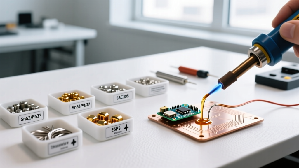
A eutectic alloy has a single, specific melting point where it transitions instantly from solid to liquid. The most famous example is Sn63/Pb37 (63% Tin, 37% Lead), which melts and freezes exactly at 183°C (361°F). Because there is no 'plastic' or semi-solid state, eutectic solders are highly forgiving. The moment you remove the heat source, the joint freezes solid, virtually eliminating the risk of disturbing the joint during the cooling phase.
Non-Eutectic Alloys: Navigating the Plastic State
Non-eutectic alloys, such as Sn60/Pb40, have a 'solidus' temperature (where melting begins) and a 'liquidus' temperature (where it is fully liquid). Sn60/Pb40 begins melting at 183°C but does not become fully liquid until 191°C. Between these two temperatures, the solder exists in a plastic, paste-like state. If a component is bumped or vibrates while the solder is in this plastic state, the internal crystalline structure fractures, resulting in a disturbed joint characterized by a dull, grainy appearance and high electrical resistance.
Comprehensive Solder Alloy Melting Temperature Matrix
The table below outlines the exact thermal thresholds for the most common solder alloys used in 2026. Note that the 'Recommended Iron Tip Temperature' accounts for the thermal loss between the iron's heating element, the tip, and the PCB joint.
| Alloy Designation | Composition | Solidus (°C) | Liquidus (°C) | Recommended Iron Tip Temp |
|---|---|---|---|---|
| Sn63/Pb37 (Leaded) | 63% Sn, 37% Pb | 183 | 183 | 300°C - 320°C |
| SAC305 (Lead-Free) | 96.5% Sn, 3.0% Ag, 0.5% Cu | 217 | 220 | 350°C - 380°C |
| SAC405 (Lead-Free) | 95.5% Sn, 4.0% Ag, 0.5% Cu | 217 | 221 | 350°C - 380°C |
| Sn42/Bi58 (Low Temp) | 42% Sn, 58% Bismuth | 138 | 138 | 220°C - 250°C |
| Sn96.5/Ag3.5 | 96.5% Sn, 3.5% Ag | 221 | 221 | 360°C - 390°C |
Source reference: Thermal data aligns with the Indium Corporation's Solder Alloy Database, a standard reference for metallurgical properties in electronics assembly.
Leaded (Sn/Pb) vs. Lead-Free (SAC): Thermal Stress on PCBs
The transition from leaded to lead-free soldering has fundamentally changed how we approach thermal management. Lead-free alloys like SAC305 require a liquidus temperature of roughly 220°C, compared to 183°C for Sn63/Pb37. This 37°C difference has profound implications for the PCB substrate and the components mounted on it.
The FR-4 Glass Transition Temperature (Tg) Limit
Standard FR-4 PCB material has a Glass Transition Temperature (Tg) ranging from 130°C to 140°C (for basic Tg130 boards) up to 170°C for high-Tg variants. When the PCB exceeds its Tg, the epoxy resin softens, and the coefficient of thermal expansion (CTE) increases dramatically, particularly in the Z-axis. Applying a 380°C iron tip to a SAC305 joint on a Tg130 board for more than 3 to 5 seconds can cause the copper pad to lift entirely off the substrate, severing the trace. This is why IPC J-STD-001 standards strictly dictate maximum dwell times and thermal exposure limits for hand soldering.
Component Thermal Shock and Micro-Cracking
Multilayer Ceramic Capacitors (MLCCs) are notoriously sensitive to rapid temperature gradients. Hitting an 0805 or 1206 MLCC pad with a 380°C chisel tip while the rest of the component is at room temperature (22°C) creates a massive thermal gradient. This stress can induce flex cracks inside the ceramic dielectric, leading to latent short-circuit failures that may not manifest until the board is deployed in the field. To mitigate this, always pre-tin one pad, let the component settle, and use the smallest tip geometry that can adequately transfer the required thermal mass.
Precision Station Calibration: Matching Iron to Alloy
Setting your soldering station to the correct temperature is not a 'set-and-forget' task. Different soldering stations utilize vastly different thermal recovery technologies, meaning a dial setting of 350°C on one brand behaves entirely differently on another.
- Hakko FX-888D / Weller WE1010NA (Standard Ceramic Heaters): These stations use a traditional ceramic heater and a separate tip sleeve. Because there is a physical air gap and thermal resistance between the heater and the tip, you must set the station roughly 30°C to 50°C higher than the actual desired joint temperature to compensate for thermal drop when touching a large ground plane. For SAC305, set the dial to 360°C - 380°C.
- JBC CD-2BE / C245 Cartridge System (Active Tip Sensing): JBC integrates the heating element and thermocouple directly inside the tip cartridge. The thermal response is near-instantaneous. Because there is zero thermal lag, you can set a JBC station roughly 30°C lower than a traditional Hakko station for the exact same result. For SAC305, a JBC setting of 320°C - 330°C is often sufficient and drastically extends tip life by reducing oxidation.
- Metcal MX-500 (Induction Heating): Metcal uses RF induction heating where the tip itself is the heater. The temperature is fixed by the Curie point of the tip's ferromagnetic core (e.g., a '5' series tip maxes out at 350°C). You cannot adjust the dial; you must physically swap the tip to change the thermal profile.
Troubleshooting Temperature-Induced Solder Defects
When the soldering lead melting temperature is mismanaged, the physical evidence is immediately visible under magnification. Here is how to diagnose and correct thermal failures:
1. The Classic 'Cold Joint'
Symptom: The solder joint appears dull, grainy, and bulbous, failing to wet properly to the component lead or pad.
Root Cause: Insufficient heat transfer. The solder wire melted against the hot iron tip, but the PCB pad and component lead never reached the liquidus temperature. The flux failed to clean the oxidation on the pad, causing the solder to ball up rather than flow.
Solution: Increase iron temperature by 20°C, use a wider tip geometry (like a bevel or larger chisel) to increase surface contact area, and apply the iron to both the pad and the lead simultaneously before feeding the solder.
2. Flux Burn-Off and Oxidized Pads
Symptom: The flux hisses violently, turns black, and leaves a hard, crusty residue. The solder refuses to flow, sticking only to the iron tip.
Root Cause: Excessive tip temperature (typically >400°C for standard rosin or no-clean fluxes). The flux activates and burns off in a fraction of a second, before it has time to chemically reduce the copper oxides on the pad.
Solution: Drop the iron temperature by 30°C. If you are forced to use high heat for massive ground planes, switch to a high-solid, high-activity water-soluble flux or apply external liquid flux directly to the joint to provide a secondary chemical cleaning buffer.
3. Pad Lifting and Delamination
Symptom: The copper pad physically separates from the fiberglass substrate, sometimes pulling the plated through-hole (PTH) barrel up with it.
Root Cause: Prolonged dwell time at high temperatures. The epoxy resin in the FR-4 has exceeded its Tg for too long, losing its structural adhesion.
Solution: Never hold an iron on a joint for more than 3-5 seconds. If the joint requires more heat due to a large thermal mass (like a power supply ground pin), use a bottom-side PCB preheater set to 100°C - 120°C. This reduces the delta-T (temperature difference) the iron must overcome, allowing you to use a lower tip temperature and shorter dwell time.
Real-World Edge Case: Soldering QFN Ground Planes
One of the most challenging scenarios involving soldering lead melting temperatures is hand-soldering the exposed thermal pad of a QFN (Quad Flat No-lead) package. The ground pad is directly connected to internal copper pours, acting as a massive heat sink.
If you attempt to solder the perimeter pins without addressing the ground pad, the heat will wick away from your iron tip into the board's inner layers, resulting in cold joints on the fine-pitch pins. The professional approach requires preheating the entire PCB to 120°C using an IR or convection preheater. Once the board is at thermal equilibrium, use a low-mass micro-pencil tip (such as a JBC C245-116) set to 320°C to quickly tack the corner pins. Finally, use a specialized hot-air rework station set to 380°C with a focused nozzle to reflow the ground pad from the top, or use a specialized thermal transfer block if the component allows. This multi-stage thermal profile ensures the soldering lead melting temperature is achieved uniformly across the entire component footprint without scorching the PCB silkscreen or damaging the silicon die inside the package.
Conclusion: Precision is Profitable
Mastering the soldering lead melting temperature is what separates amateur tinkerers from professional electronics engineers. By selecting the correct alloy for your application, understanding the metallurgical properties of eutectic versus non-eutectic transitions, and calibrating your specific soldering station to compensate for thermal mass, you ensure long-term reliability. Whether you are working with legacy Sn63/Pb37 aerospace hardware or assembling modern SAC305 IoT devices, respecting the thermal limits of your materials is the foundation of flawless PCB assembly.