
The PCB Soldering Decision Framework
When soldering electronic circuit boards, the margin for error shrinks exponentially as component pitch decreases and multilayer ground planes increase in thermal mass. A generic approach to PCB assembly inevitably leads to cold joints, tombstoning, or catastrophic pad delamination. To achieve consistent, high-yield results, engineers and technicians must adopt a structured decision framework. This guide provides a comprehensive, step-by-step methodology for selecting the right thermal tools, metallurgical alloys, and chemical fluxes based on your specific board architecture and production environment.
Phase 1: Component Density & Thermal Mass Assessment
Before selecting a soldering station, you must audit the board's physical characteristics. The primary decision driver is the ratio of surface-mount device (SMD) density to through-hole technology (THT) components, coupled with the copper weight of the internal layers.
- Low-Density THT & Large SMD (0805+): Standard hobbyist or repair boards. Thermal mass is low, and pad sizes are forgiving. Basic temperature-controlled irons are sufficient.
- High-Density SMD (0603, 0402, QFN): Modern microcontrollers and RF modules. Requires precise tip geometry, rapid thermal recovery, and specialized tacky fluxes to prevent component shifting.
- Heavy Copper Multilayer (4+ layers, 2oz+ copper): Power electronics and motor controllers. These boards act as massive heatsinks, drawing heat away from the joint faster than standard irons can replenish it, requiring high-wattage active-tip systems or localized preheating.
Phase 2: Soldering Station Selection Matrix
Choosing the right heat source is the most critical capital expenditure in your workflow. The market in 2026 offers distinct tiers based on thermal recovery technology. Below is a decision matrix to match your board assessment with the optimal hardware.
| Station Model | Price Range | Wattage & Tech | Best Use Case | Limitations |
|---|---|---|---|---|
| Pinecil V2 | $26 - $35 | 65W (RISC-V PID) | Prototyping, 0805+ SMD, basic THT, field repairs. | Struggles with heavy ground planes; tip thermal mass is low. |
| Hakko FX-888D | $105 - $120 | 70W (Ceramic Heater) | General THT, DIP ICs, large connectors, standard SMD. | Slow thermal recovery on large pads; T18 tips lack micro-precision. |
| Weller WE1010NA | $115 - $130 | 70W (ET Series) | Educational labs, mixed THT/SMD boards, continuous daily use. | Tip changes require cooling or specialized tools. |
| JBC CD-2BQE | $485 - $520 | 130W (Cartridge) | 0402 SMD, QFN/BGA rework, heavy multilayer power boards. | High initial cost; proprietary cartridge ecosystem. |
The Expert Verdict: If your workflow involves soldering electronic circuit boards with 0402 imperial components (1.0mm x 0.5mm) or dense QFN packages, bypass the Hakko and Weller mid-tier options. The JBC C245 cartridge system integrates the heating element directly into the tip, achieving a 2-second thermal recovery time that prevents the operator from lingering on sensitive pads, thereby protecting the underlying FR4 substrate.
Phase 3: Metallurgical & Chemical Decisions
The physical connection relies on the intermetallic compound (IMC) layer formed between the copper pad and the solder alloy. Your choice of alloy and flux must align with your operational constraints and environmental compliance requirements.
Solder Alloy Decision Guide
Selecting the right wire diameter and core composition is non-negotiable. For 0603 and 0402 SMD work, use 0.3mm to 0.5mm diameter wire. For standard THT, 0.8mm to 1.0mm is optimal.
- Sn63/Pb37 (Eutectic Leaded): Melts at exactly 183°C. It transitions instantly from solid to liquid with no plastic state, eliminating cold-joint risks caused by micro-movements during cooling. Decision: Choose for prototyping, hobbyist, and non-RoHS commercial repair.
- SAC305 (Sn96.5/Ag3.0/Cu0.5): The industry-standard lead-free alloy. Melts between 217°C and 220°C. Requires higher iron temperatures (typically 350°C+) and exhibits a grainy finish that novices often mistake for a cold joint. Decision: Mandatory for RoHS-compliant commercial production and medical device assembly.
- Sn99.3/Cu0.7 (Lead-Free Economy): Melts at 227°C. Lacks silver, making it cheaper but significantly reducing wetting speed and increasing the required dwell time on the pad. Decision: Best for high-volume, cost-sensitive THT wave-soldering or manual heavy-gauge wire tinning.
Flux Chemistry Matrix
Flux removes copper oxidation and reduces surface tension. Using the wrong flux chemistry will either destroy your board over time or result in non-wetting pads.
Pro Tip: Never use plumbing acid flux on PCBs. The chloride ions will rapidly corrode copper traces and create dendritic shorts under voltage bias. Always stick to electronics-grade Rosin or synthetic organic acids.
| Flux Type | Activation Temp | Residue Cleanup | Recommended Product (2026) |
|---|---|---|---|
| Rosin Mildly Activated (RMA) | 150°C - 180°C | Requires Isopropyl Alcohol (IPA) | Kester 186 Liquid / 245 Wire Core |
| No-Clean (Synthetic) | 180°C - 220°C | Leave on board (non-conductive) | Amtech NC-559-V2-TF (Tacky SMD) |
| Water-Soluble (Organic Acid) | 160°C - 200°C | Mandatory DI Water Wash | MG Chemicals 8341 |
Phase 4: Thermal Execution & Wetting Logic
Executing the solder joint requires a precise understanding of thermal transfer. According to the rigorous guidelines outlined in NASA-STD-8739.3 for soldered electrical connections, a proper joint relies on capillary action and specific wetting angles. The solder must flow smoothly up the component lead, forming a concave fillet with a wetting angle of less than 90 degrees.
- Preparation: Apply a microscopic amount of flux to the pad. If using a lead-free alloy, ensure your station is set to 340°C - 360°C. For Sn63/Pb37, set to 315°C - 325°C.
- Tinning the Tip: Always apply a small dab of solder to the iron tip immediately before contact. This creates a 'thermal bridge' that drastically increases heat transfer efficiency compared to a dry, oxidized tip.
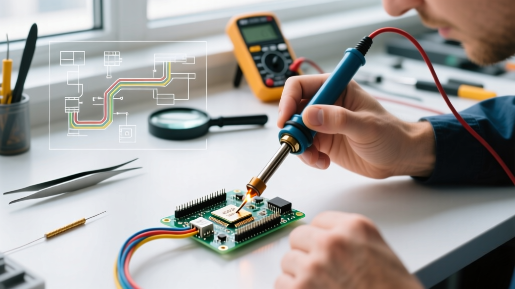
- Simultaneous Heating: Place the tinned tip so it contacts BOTH the component lead and the PCB pad simultaneously. Hold for 1 to 1.5 seconds.
- Feed the Solder: Introduce the solder wire to the opposite side of the pad/lead, not directly onto the iron tip. The solder should melt from the heat of the workpiece, proving that the joint has reached flow temperature.
- Withdrawal: Remove the solder wire first, then sweep the iron tip away at a 45-degree angle to leave a clean, concave fillet. Do not blow on the joint; forced cooling creates micro-fractures in the IMC layer.
Edge Cases & Failure Mode Troubleshooting
Even with the right tools, environmental and mechanical variables can introduce defects. The IPC J-STD-001 standard categorizes these defects by severity. Here is how to diagnose and resolve the most common framework failures:
1. Tombstoning (Drawbridging) on SMD
The Symptom: A two-terminal SMD component (like a 0603 resistor) stands up on one end, soldered to only a single pad.
The Root Cause: Uneven heating. If the iron tip touches one pad slightly before the other, or if one pad is connected to a massive ground plane while the other is a thin signal trace, the solder on the hotter pad melts first. The surface tension of the liquid solder pulls the component upright.
The Fix: Use a chisel tip to bridge both pads simultaneously, or apply solder paste and use a hot air rework station for uniform heating.
2. Pad Delamination & Lifting
The Symptom: The copper pad separates from the fiberglass FR4 substrate, sometimes tearing the trace entirely.
The Root Cause: Excessive dwell time. Standard FR4 has a Glass Transition Temperature (Tg) between 130°C and 170°C. Holding a 380°C iron on a pad for more than 4 seconds degrades the epoxy resin bond.
The Fix: If a joint isn't flowing within 3 seconds, remove the heat. Add more flux, increase the iron temperature slightly, or switch to a higher-wattage station with better thermal recovery rather than holding a cooler iron on the pad longer.
3. Icy or Disturbed Joints
The Symptom: The solder joint appears dull, grainy, or cracked.
The Root Cause: For Sn63/Pb37, this is a 'disturbed joint' caused by physical movement before solidification. For SAC305, a grainy appearance is actually the natural crystalline structure of lead-free solder, but true cold joints will show visible cracks or poor wetting (beading up like water on wax).
The Fix: Secure the board in a PCB vise or use a third-hand tool. If using SAC305, ensure the flux core is fully activated by maintaining adequate heat dwell time.
Health, Safety, and Environmental Compliance
Soldering electronic circuit boards generates colophony fumes (from rosin flux) and, if using leaded alloys, poses a heavy metal exposure risk. The Occupational Safety and Health Administration (OSHA) strictly regulates lead handling in occupational settings. Lead does not vaporize at soldering temperatures (lead boils at 1749°C); the risk comes from touching contaminated surfaces and ingesting it via hand-to-mouth contact.
Safety Framework Mandates:
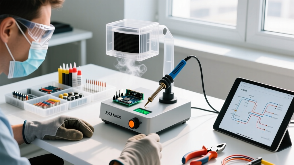
- Always utilize a localized fume extractor with a HEPA and activated carbon filter positioned within 6 inches of the solder joint to capture rosin particulates and volatile organic compounds (VOCs).
- Implement a strict hand-washing protocol before eating or drinking when handling Sn63/Pb37 solder.
- Dispose of water-soluble flux wash water and lead-contaminated wipes according to local hazardous electronic waste (e-waste) regulations.
Final Synthesis
Successfully soldering electronic circuit boards is not merely a manual skill; it is an applied science of thermodynamics and metallurgy. By utilizing this decision framework—accurately assessing board density, investing in active-tip thermal recovery systems for dense SMD work, matching alloy chemistry to your compliance needs, and adhering to strict wetting execution protocols—you will eliminate guesswork and achieve professional-grade, highly reliable PCB assemblies every time.