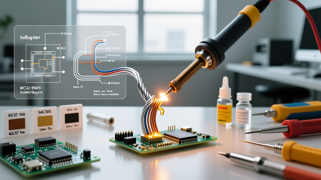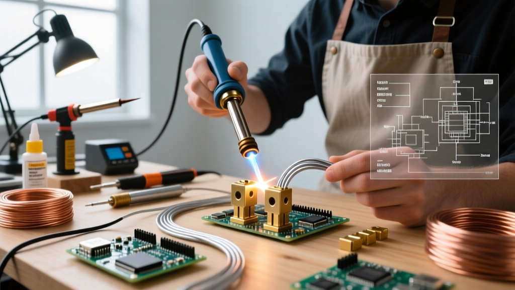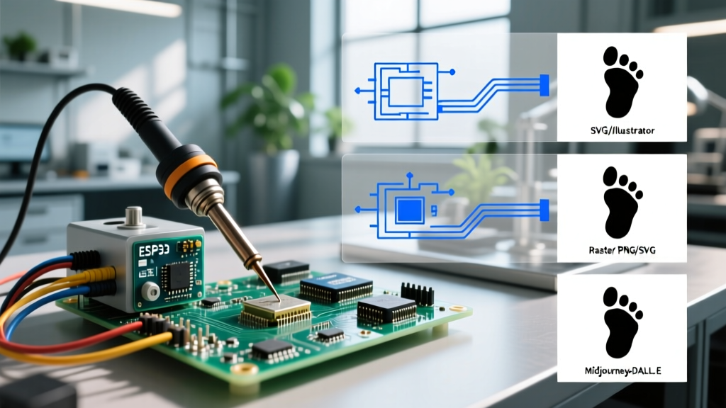

The Evolution of Electronics Illustration: Why Soldering Clipart Matters
In the realm of electronics manufacturing, technical documentation, and PCB design, visual communication is just as critical as the schematic itself. When engineers and technical writers search for soldering clipart, they are rarely looking for cartoonish illustrations. Instead, they require precise, scalable, and accurate graphical representations of solder joints, iron tips, PCB footprints, and assembly processes. Whether you are designing a silkscreen layer for a custom PCB in KiCad, writing an IPC-compliant assembly manual, or creating educational DIY guides, the method you use to source and generate this graphics dictates your final output quality.
As of 2026, the landscape of technical illustration has fractured into four distinct methodologies: traditional Vector graphics, high-DPI Raster images, AI-generated conceptual art, and direct ECAD parametric exports. This buyer's guide and method comparison will break down the costs, technical limitations, and ideal use cases for each approach, helping you choose the right workflow for your next electronics project.
Method 1: Vector Graphics (SVG/EPS) – The Silkscreen Standard
Vector graphics use mathematical formulas to render lines and shapes, meaning they can be scaled infinitely without losing resolution. For PCB silkscreen design and high-quality print manuals, vector-based soldering clipart is the undisputed industry standard.
Pros and Cons of Vector Workflows
- Pros: Infinite scalability; native compatibility with ECAD tools (KiCad, Altium, Eagle); easily editable line weights; small file sizes.
- Pros: Perfect for silkscreen layers where minimum line widths (typically 0.15mm or 6 mil) must be strictly maintained.
- Cons: Steep learning curve for software like Adobe Illustrator; cannot capture photorealistic textures of actual solder joints.
Cost Analysis: You can use Inkscape (Free, Open Source) or Adobe Illustrator ($22.99/month). For most DIYers and small engineering firms, Inkscape provides all the necessary SVG export capabilities required for PCB import.
Method 2: Raster Images (PNG/TIFF) – The Web Tutorial Workhorse
Raster images are pixel-based. When sourcing soldering clipart for web-based tutorials, blog posts, or quick-reference PDF guides, high-resolution PNGs with transparent backgrounds are the most common format. However, they fail entirely in CAD environments.
Technical Specifications for Raster Clipart
If you are buying or downloading raster soldering clipart for print documentation, you must enforce strict resolution requirements. According to IEEE technical documentation standards, print graphics require a minimum of 600 DPI at the final physical print size. For web-only guides, 144 DPI is sufficient to maintain crispness on Retina and high-DPI mobile displays.
Expert Warning: Never attempt to import a PNG or JPG into a PCB silkscreen layer. ECAD software will either reject the file, or convert it into a massive array of individual vector lines that will crash your board's DRC (Design Rule Check) and cause manufacturing failures at the fab house.
Method 3: AI-Generated Soldering Clipart – The 2026 Frontier
With the maturation of generative AI models like Midjourney v6.1 and DALL-E 3, many technical writers are turning to AI to generate custom soldering clipart. While AI excels at creating striking, conceptual header images for articles (e.g., 'a glowing cyberpunk soldering iron on a workbench'), it remains highly problematic for precise technical diagrams.
The Hallucination Problem in Electronics Art
AI models do not understand electrical engineering principles. If you prompt an AI for 'soldering clipart of an SOIC-8 footprint,' the model will likely hallucinate the pin count, misalign the ground plane, or generate physically impossible solder joint geometries. Therefore, AI-generated clipart should be strictly limited to conceptual and decorative uses, never for schematic symbols, PCB footprints, or step-by-step wiring diagrams where exact pinouts are required.
Cost Analysis: Midjourney Standard Plan ($30/month) offers commercial rights and high-resolution upscaling, making it a viable purchase for content creators needing unique blog graphics without relying on generic stock photo sites.
Method 4: ECAD Parametric Export – The Engineer's Choice
The most accurate 'clipart' for soldering and assembly documentation doesn't come from a stock library; it comes directly from your 3D ECAD models. Modern software like Altium Designer and KiCad 8 allow engineers to export 2D vector projections of their 3D PCB assemblies.
By exporting a DXF or SVG from the 3D viewer, you generate 100% accurate, to-scale clipart of your specific board, complete with exact component placements and silkscreen outlines. This method is heavily endorsed by the Open Source Hardware Association (OSHW) for creating open-source assembly manuals, as it guarantees that the documentation perfectly matches the manufactured board revision.
Method Comparison Matrix
| Method | Primary Formats | ECAD Compatibility | Accuracy for Pinouts | Best Use Case | Estimated Cost |
|---|---|---|---|---|---|
| Vector (Manual) | SVG, EPS, DXF | Excellent (Native) | High (If drafted correctly) | PCB Silkscreens, Print Manuals | $0 - $23/mo |
| Raster (Stock) | PNG, JPG, TIFF | None | Low to Medium | Web Tutorials, Blog Headers | $10 - $30/mo |
| AI-Generated | PNG, JPG | None | Extremely Low (Hallucinated) | Conceptual Art, Marketing | $10 - $30/mo |
| ECAD Export | SVG, DXF, PDF | Perfect (Source) | Absolute (1:1 Scale) | Assembly Guides, Datasheets | Included in ECAD |
Step-by-Step: Importing Vector Soldering Clipart into KiCad 8
If you have sourced or created vector-based soldering clipart (such as a company logo, a custom warning symbol, or a graphical soldering iron icon for a DIY kit silkscreen), follow these steps to implement it correctly in KiCad 8:
- Prepare the SVG: Open your graphic in Inkscape. Convert all text to paths (Path > Object to Path) and ensure all strokes are converted to fills. ECAD tools struggle with raw stroke lines.
- Set Dimensions: Scale your graphic to the exact physical dimensions required on the PCB (e.g., 10mm x 10mm). Set the document units to millimeters.
- Check Line Widths: Verify that the thinnest part of your clipart is at least 0.15mm (6 mil). Anything thinner may be lost during the standard PCB manufacturing silkscreen printing process.
- Import to KiCad: Open the PCB Editor in KiCad. Navigate to File > Import > Graphics.
- Assign Layer: Select the
F.SilkS(Front Silkscreen) orB.SilkS(Back Silkscreen) layer. Do not import graphics onto the copper layers (F.Cu) unless you specifically intend to create a custom copper pour shape. - Run DRC: Press F8 to run the Design Rules Checker to ensure your imported clipart does not violate clearance rules with nearby pads or vias.
Frequently Asked Questions (FAQ)
Can I use standard clipart libraries for commercial PCB manufacturing?
It depends entirely on the licensing. Many free clipart sites offer 'Personal Use Only' licenses. If you are manufacturing a PCB for a commercial product, you must source graphics from platforms that provide explicit Commercial or CC0 (Public Domain) licenses. Always verify the license before sending your Gerber files to a fab house.
Why does my soldering clipart look jagged on the finished PCB?
This is usually a result of using raster images converted to vectors via auto-trace, or using vector lines that are too thin. Standard silkscreen printing uses a mesh screen that cannot resolve ultra-fine details. Ensure your vector paths are fully closed and possess a minimum fill width of 0.15mm to guarantee clean ink deposition.
Is AI clipart safe to use in open-source hardware documentation?
While you can use AI for decorative elements, using AI-generated diagrams for actual wiring or soldering instructions in open-source hardware is highly discouraged. The OSHW community prioritizes reproducibility and accuracy; hallucinated AI diagrams will lead to user frustration, short circuits, and damaged components. Stick to ECAD exports and manual vector drafting for technical accuracy.