
The Permanent Bond: When Components Are Soldered On
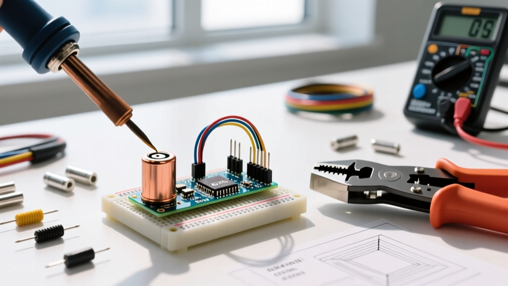
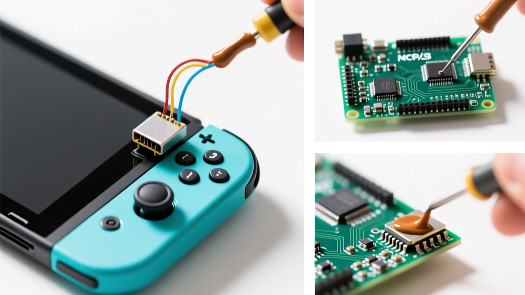
In the realm of printed circuit board (PCB) assembly and electronics manufacturing, the method used to attach components to the board dictates the product's long-term reliability, manufacturing cost, and serviceability. When a component is soldered on, it forms a permanent metallurgical bond with the copper pads or plated through-holes (PTH) of the PCB. While this is the default approach for the vast majority of consumer and industrial electronics, it is not universally the best choice for every application.
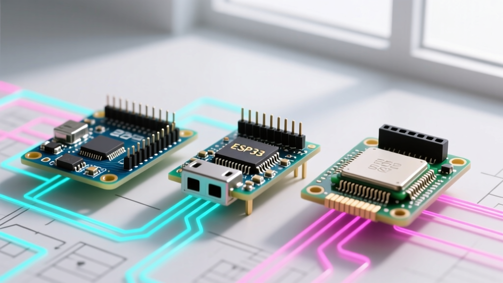
As we navigate the manufacturing landscape in 2026, engineers must weigh the traditional "soldered on" approach against advanced solderless alternatives like press-fit technology and modular socketed connections. This guide provides a deep-dive comparison of these three primary PCB connection methods, analyzing thermal stresses, mechanical failure modes, capital equipment costs, and industry standards.
The Metallurgical Reality of Soldered Connections
When a component is soldered on, the solder alloy melts, wets the copper surfaces, and forms intermetallic compounds (IMCs)—typically Cu6Sn5 and Cu3Sn in tin-copper systems. This IMC layer is the actual electrical and mechanical bridge between the component lead and the PCB pad.
Thermal Profiles and Alloy Selection
The most common lead-free alloy used in modern commercial manufacturing is SAC305 (96.5% Tin, 3.0% Silver, 0.5% Copper). SAC305 has a melting point of 217°C. To achieve proper wetting and IMC formation, the reflow or wave soldering process must push the peak temperature to approximately 240°C–245°C, maintaining a Time Above Liquidus (TAL) of 45 to 60 seconds.
- Ramp-to-Spike Profile: Heats the board rapidly to minimize overall thermal exposure, ideal for simple boards with low thermal mass variations.
- Soak Profile: Holds the board at 150°C–175°C for 60–90 seconds before the final reflow spike, ensuring thermal equilibrium across complex boards with heavy copper pours and mixed BGA/QFN components.
For aerospace, military, and certain medical devices where lead-free mandates do not apply, Sn63Pb37 (63% Tin, 37% Lead) remains the gold standard. Its eutectic melting point of 183°C results in significantly lower thermal stress on the PCB laminate and components during the soldering process. According to the IPC-A-610 standard, Class 3 requirements for high-reliability soldered joints demand specific fillet shapes, complete wetting, and an absence of cold solder defects or excessive voiding in bottom-terminated components (BTCs).
The Solderless Challenger: Press-Fit Technology
Press-fit technology eliminates the soldering process entirely for specific connectors and pins. Instead of melting an alloy, a compliant pin is mechanically forced into a plated through-hole (PTH). The pin is slightly larger than the hole, causing the pin's compliant section (such as an "eye of the needle" or "action pin" design) to deform and press tightly against the copper barrel of the PTH.
Mechanical Realities and Tooling
Press-fit connections rely on cold welding and extreme friction to create a gas-tight, low-resistance electrical contact. Because no heat is applied, the PCB laminate and surrounding surface-mount components are completely spared from thermal degradation.
However, the mechanical forces involved are immense. Inserting a high-pin-count backplane connector might require a total insertion force of several thousand Newtons. This necessitates precision arbor presses or automated servo-driven press-fit machines equipped with force-displacement monitoring to ensure no pins are bent and no PTH barrels are cracked during insertion.
Modularity at a Cost: Socketed Connections
Socketed connections involve soldering a receptacle (the socket) to the PCB, and then plugging the actual component or daughterboard into the socket. This is common for microcontrollers (using DIP or LGA sockets), FPGAs, and modular board-to-board connectors.
The primary advantage is reworkability and modularity. If a $500 FPGA fails or requires a firmware-level hardware swap, it can be removed without applying heat to the PCB. However, every socket introduces a mechanical interface prone to environmental degradation. According to reliability data from the NASA Electronic Parts and Packaging (NEPP) program, mechanical contacts are inherently more susceptible to fretting corrosion, oxidation, and vibration-induced micro-disconnects than permanent metallurgical bonds.
Head-to-Head PCB Connection Matrix
To visualize the engineering trade-offs, review the comparison matrix below detailing the physical and economic characteristics of each method.
| Characteristic | Soldered On (SMT/THT) | Press-Fit Compliant Pin | Socketed / Plug-In |
|---|---|---|---|
| Bond Type | Metallurgical (Intermetallic Compound) | Mechanical (Cold Weld / Friction) | Mechanical (Spring Contact) |
| Thermal Stress to PCB | High (up to 245°C peak) | None (Room temperature) | Moderate (Socket is soldered on) |
| Vibration Resistance | Excellent (Permanent mass) | Excellent (Rigid interference fit) | Poor to Fair (Susceptible to resonance) |
| Reworkability | Difficult (Requires localized heat) | Moderate (Requires extraction tools) | Excellent (Zero Insertion Force options) |
| Primary Failure Mode | Thermomechanical fatigue / Solder cracking | PTH barrel cracking / Plating wear | Fretting corrosion / Contact oxidation |
| Relative BOM Cost | Lowest (Direct attachment) | Low (No solder, but specialized pins) | Highest (Socket adds $0.50 - $5.00+) |
Real-World Failure Modes and Edge Cases
Understanding how these connections fail in the field is critical for design engineers. The Surface Mount Technology Association (SMTA) frequently publishes case studies highlighting these exact failure mechanisms.
When Soldered On Fails
The most common failure for components that are soldered on is thermomechanical fatigue. Because the component body (e.g., silicon or ceramic) and the PCB laminate (e.g., FR4) have different Coefficients of Thermal Expansion (CTE), temperature cycling causes the solder joints to shear. Over thousands of cycles, micro-cracks initiate at the IMC layer and propagate through the bulk solder, eventually leading to an open circuit. Edge cases include tin whisker growth in pure tin finishes, which can cause catastrophic short circuits in high-voltage or high-impedance analog circuits.
Press-Fit and Socketed Failures
Press-fit failures usually occur during the manufacturing phase rather than in the field. If the PTH diameter tolerance is off by even 0.02mm, the insertion force can crack the copper barrel or delaminate the inner layers of the PCB. In the field, socketed connections suffer from fretting corrosion. Micro-vibrations cause the pin to rub against the socket contact, wearing away the gold flash and exposing the underlying nickel or copper to oxygen, which rapidly increases contact resistance and causes signal integrity degradation in high-speed data lines.
Capital Equipment and Cost Analysis
The decision to have a component soldered on versus using alternative methods heavily impacts the manufacturing floor's capital expenditure (CapEx).
- Soldering Equipment: A high-end selective soldering machine (for complex THT components that cannot endure wave soldering) costs between $65,000 and $120,000. A multi-zone reflow oven for SMT ranges from $15,000 to $45,000. Furthermore, the ongoing cost of solder paste, flux, and nitrogen gas generation adds to the operational expenditure (OpEx).
- Press-Fit Equipment: A manual arbor press with a digital force gauge costs around $2,000. However, automated, servo-driven press-fit machines with closed-loop force-displacement monitoring—required for high-volume telecom backplanes—cost between $40,000 and $80,000. The OpEx is significantly lower, as no solder, flux, or post-assembly cleaning is required.
- Socketed Assembly: Requires minimal assembly equipment (often just manual insertion or light robotic pick-and-place), but drastically inflates the Bill of Materials (BOM). A high-speed LGA socket for a modern processor can add $4.00 to $12.00 per unit to the BOM, which is prohibitive for high-volume consumer goods.
Expert Insight: Never use a socket purely for the sake of reworkability on a high-speed digital interface (e.g., PCIe Gen 5 or DDR5 memory) unless the system architecture demands field-replaceable modules. The parasitic inductance and capacitance introduced by the socket's spring contacts will degrade signal integrity and shrink timing margins far more than a direct soldered connection.
Expert Verdict: Designing for Reliability
The choice between having a component soldered on, press-fit, or socketed is not a matter of one being universally superior; it is an exercise in matching the connection physics to the product's lifecycle and environment.
Choose the "Soldered On" method when: You are designing high-volume consumer electronics, automotive ECUs, or high-speed digital boards where signal integrity, minimal parasitic inductance, and low BOM costs are paramount. Ensure your thermal profiles are optimized to prevent CTE-induced fatigue.
Choose Press-Fit when: You are assembling heavy backplane connectors, high-current power terminals, or thick multi-layer boards (12+ layers) where the thermal mass would make wave or selective soldering incredibly difficult and prone to cold solder defects.
Choose Socketed when: You are building test-and-measurement equipment, modular server architectures, or prototype boards where the cost of the socket is easily justified by the ability to upgrade or replace multi-thousand-dollar silicon chips without scrapping the entire PCB assembly.
By understanding the metallurgical, mechanical, and economic realities of these three methods, electrical engineers can design PCBs that not only function perfectly on the test bench but survive the harsh realities of deployment in 2026 and beyond.