
The Role of Solderability Testing in Material Compatibility
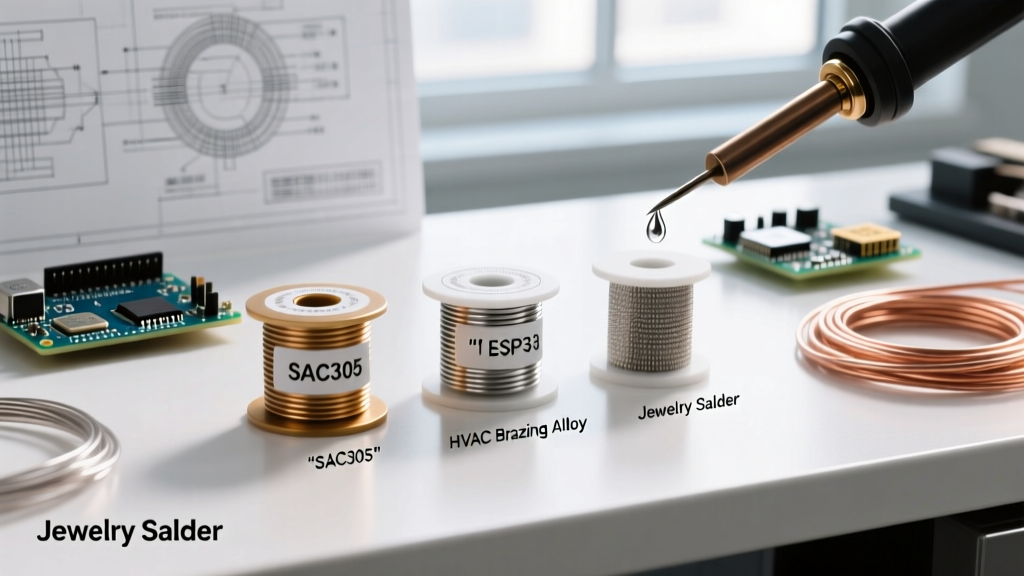
In high-reliability electronics manufacturing, the interface between a component termination and a printed circuit board (PCB) pad is a critical failure point. Solderability testing is not merely a quality control checkbox; it is a fundamental material compatibility assessment. As the industry transitions toward more complex lead-free alloys like SAC305 (Tin-Silver-Copper) and SN100C (Tin-Copper-Nickel), understanding how different surface finishes and base metals interact with molten solder is paramount. Poor material compatibility manifests as non-wetting, dewetting, tombstoning, or catastrophic intermetallic compound (IMC) fracturing under thermal cycling.
This guide explores the mechanics of solderability testing from a material compatibility perspective, detailing how to evaluate surface finishes, select the right testing methodology, and invest in precision equipment for your lab or production floor.
Decoding the IPC Standards: J-STD-002 vs. J-STD-003
Before selecting a testing method, you must align your procedures with established industry benchmarks. The IPC J-STD-002 and J-STD-003 standards form the backbone of global solderability qualification.
- IPC J-STD-002: Governs solderability tests for component leads, terminations, lugs, terminals, and wires. It focuses on the component side of the material interface, evaluating how well the lead finish (e.g., matte tin, silver, or gold) wets under specific flux and temperature conditions.
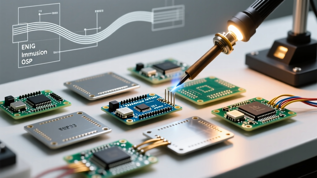
- IPC J-STD-003: Specifically targets solderability tests for printed boards. It evaluates the PCB surface finish (ENIG, HASL, OSP, Immersion Silver) and the integrity of the plated through-holes (PTH).
For aerospace and defense applications, engineers often cross-reference these with the NASA Electronic Parts and Packaging (NEPP) program guidelines and NASA-STD-8739.3, which demand stricter wetting percentages and zero-tolerance for dewetting on Class 3 hardware.
Core Testing Methodologies: A Comparative Matrix
Choosing the right test depends on the physical geometry of the material being tested and the quantitative data required. Below is a comparison of the three primary methodologies used in modern material compatibility labs.
| Methodology | Best For | Data Output | Equipment Cost Range | Material Limitations |
|---|---|---|---|---|
| Dip and Look | Standard PCB pads, large component leads, PTH barrels | Qualitative (Visual % coverage) | $1,500 - $4,500 | Cannot test ultra-fine pitch (<0.4mm) reliably |
| Wetting Balance | Quantitative alloy research, IMC formation studies | Quantitative (Force in mN vs. Time in seconds) | $18,000 - $35,000 | Requires precise sample fixturing; sensitive to vibration |
| Solder Globule | Ultra-fine pitch SMDs, micro-BGAs, fragile terminations | Semi-Quantitative (Time to envelopment) | $8,000 - $15,000 | Not suitable for large through-hole components |
Material Compatibility Matrix: How PCB Finishes React
The core of material compatibility lies in how the PCB surface finish interacts with the solder alloy and the flux chemistry. Each finish presents unique metallurgical challenges during solderability testing.
1. ENIG (Electroless Nickel Immersion Gold)
ENIG provides a remarkably flat surface, ideal for fine-pitch BGAs. During testing, the thin gold flash (typically 0.05µm to 0.1µm) dissolves into the molten solder in less than 0.5 seconds. The actual wetting and IMC formation occur on the electroless nickel layer. Edge Case: If the nickel bath was contaminated during PCB fabrication, 'black pad syndrome' (hyper-corrosion of the nickel) can occur. Solderability testing will reveal this as catastrophic non-wetting or brittle fractures, even if the gold surface looks pristine to the naked eye.
2. HASL (Hot Air Solder Leveling)
Lead-free HASL (usually SAC305 or SN100C) is essentially pre-tinned. Solderability testing on HASL is generally a pass, provided the board hasn't oxidized due to improper storage. However, because the surface is inherently uneven, meniscograph (wetting balance) readings can show high variance in maximum wetting force (Fmax) due to the inconsistent surface area contacting the solder bath.
3. Immersion Silver (ImAg)
Immersion silver offers excellent solderability and a flat surface but is highly susceptible to sulfur-induced tarnishing and creep corrosion. When performing solderability testing on ImAg boards that have been exposed to ambient air for more than 48 hours, you must use a mildly activated rosin flux (ROM1) rather than a standard ROL0 to break through the silver sulfide layer. Testing in a nitrogen-inerted chamber is highly recommended for baseline material qualification.
4. OSP (Organic Solderability Preservative)
OSP is a thin organic layer that protects the underlying bare copper. It does not dissolve in solder; it must be chemically displaced by the flux. If your solderability test yields non-wetting results on OSP, the failure is rarely the copper itself—it is usually a flux activation failure. Ensure your test flux reaches its activation temperature (typically 150°C–180°C) before the sample hits the 255°C solder pot.
Selecting Solderability Testing Equipment
Investing in the right equipment requires matching the machine's sensitivity to your material compatibility goals. According to Circuit Insight reliability testing protocols, quantitative data is increasingly required for automotive (AEC-Q100) and medical device qualifications.
Wetting Balance Testers: Rhesca vs. Malcom
For labs requiring precise force-over-time measurements to study IMC growth rates, a wetting balance is mandatory.
- Rhesca SAT-5200T: Priced between $24,000 and $28,000, this unit is renowned for its high-resolution load cell (0.1mN resolution) and integrated atmospheric control options. It is the preferred choice for aerospace labs analyzing the exact millisecond of flux breakthrough on ENIG finishes.
- Malcom ST-100 Series: Coming in at $18,000 to $22,000, Malcom offers a robust, slightly more compact alternative. It excels in high-throughput dip-and-look and wetting balance combo testing, making it ideal for high-volume PCB fabrication houses running daily batch validations.
Static Solder Pots for Dip-and-Look
For standard IPC J-STD-003 compliance, a static solder pot is sufficient. However, dross accumulation severely skews material compatibility results by introducing oxide inclusions into the wetting interface. Budget $2,500 to $4,000 for a digitally controlled static pot with a ceramic heating element to prevent localized hot spots. Always use a dross-reducing compound (like Kester Drossex) and skim the pot immediately before every test cycle.
Expert Callout: The Flux Variable
Never use the same flux for testing all materials. A standard ROL0 (Rosin, Low-activity, 0% halides) flux is perfect for testing fresh HASL or gold finishes. However, if you are evaluating the solderability of aged matte-tin component leads or slightly oxidized OSP, you must switch to an ORL1 (Organic, Low-activity, 1% halides) flux to accurately determine if the base metal is still viable beneath the oxidation layer.
Troubleshooting Common Wetting Failures
When a material fails solderability testing, diagnosing the root cause requires distinguishing between three distinct visual and mechanical phenomena:
- Non-Wetting: The solder retracts, leaving the base metal exposed. This indicates a fundamental material incompatibility, severe oxidation, or a missing barrier layer (e.g., copper diffusion into the finish).
- Dewetting: The solder initially coats the surface but then pulls back into islands or beads as it cools, leaving a thin, uneven film. This is a classic signature of IMC instability or contamination (such as silicone residue or incorrect plating bath chemistry).
- Slow Wetting: The solder eventually covers the pad, but the wetting time exceeds the 2-second IPC threshold. This usually points to an overly thick finish (e.g., >0.15µm gold) which lowers the localized temperature of the solder meniscus, or a flux that is under-activated.
Frequently Asked Questions (FAQ)
How long can PCBs be stored before solderability testing is required?
Standard industry practice dictates that HASL and ENIG boards can be stored for up to 12 months in a controlled environment (25°C, <10% RH). Immersion Silver and OSP boards have a much shorter shelf life of 3 to 6 months. If boards exceed these windows, a baseline dip-and-look test per IPC J-STD-003 is mandatory before releasing them to the SMT line.
Does the solder pot alloy need to match the PCB finish?
Not necessarily, but it must match your final production process. If you are testing the material compatibility of an ENIG board for a lead-free assembly, the test pot must contain a lead-free alloy like SAC305 at 255°C ± 5°C. Testing a lead-free board in a Sn63/Pb37 pot at 245°C will yield false-pass results due to the lower surface tension and higher fluidity of leaded solder.
Can X-Ray fluorescence (XRF) replace solderability testing?
No. XRF is a critical tool for measuring the thickness of surface finishes (e.g., verifying that ENIG gold is exactly 0.05µm). However, XRF cannot detect organic contamination, oxide formation, or 'black pad' nickel corrosion. Solderability testing remains the only definitive method to prove functional material compatibility.