
The Reality of Lifted Pads and IPC Standards
Lifted or detached PCB pads are among the most catastrophic failures encountered during electronics rework. Typically caused by excessive thermal profiling (exceeding 380°C for more than 3 seconds) or mechanical shear stress during component desoldering, a lifted pad breaks the electrical continuity and compromises the structural integrity of the board. When executing repair pad soldering work, technicians must choose a restoration method that satisfies both electrical conductivity and mechanical tensile strength requirements.
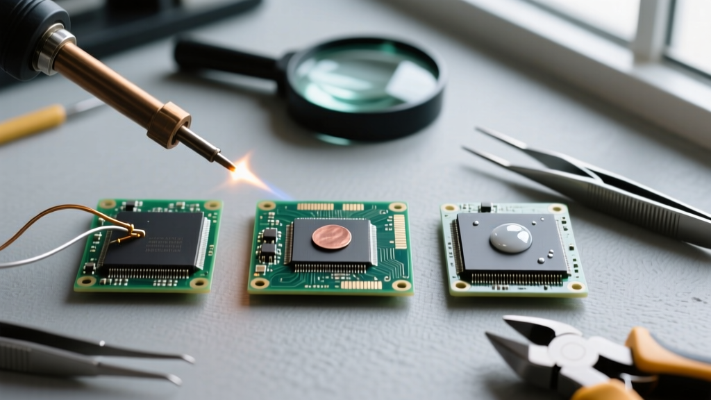
According to the IPC-7711/7721 standard for rework, modification, and repair of electronic assemblies, any pad replacement must restore the original electrical function and withstand the mechanical stresses of the final operating environment. In 2026, with the proliferation of high-density interconnect (HDI) boards and micro-BGA packages, the margin for error in pad repair has shrunk to fractions of a millimeter. Below, we compare the three primary methodologies for pad restoration: wire jumping, copper tape/dots, and conductive silver epoxy.
Method 1: Wire Jumping (Flying Wires)
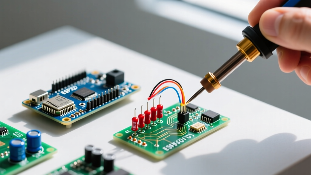
Wire jumping involves bypassing the damaged pad and trace entirely by soldering a fine-gauge insulated wire directly from the component lead to the next viable test point or via.
Technique & Specifications
- Material: 30 AWG or 32 AWG Kynar or PTFE insulated solid-core wire. Kynar is preferred for its high melting point (prevents insulation shrinkback during soldering).
- Solder Alloy: Sn63/Pb37 for legacy boards, or SAC305 (Sn96.5/Ag3.0/Cu0.5) for RoHS-compliant 2026 assemblies.
- Thermal Profile: Iron tip temperature set to 320°C–340°C. Dwell time must not exceed 2 seconds per joint to prevent underlying fiberglass delamination.
- Cost: Approximately $18 to $25 for a 100-foot spool of 30 AWG Kynar wire.
Pros & Cons
Pros: Offers the highest mechanical tensile strength and lowest electrical resistance. It is the only method universally accepted for aerospace and military Class 3 assemblies under NASA-STD-8739.3 workmanship requirements.
Cons: Requires high manual dexterity and advanced micro-soldering skills. Routing the wire can interfere with nearby components or heat sinks, and the repair is highly visible.
Method 2: Copper Tape and Pre-Cut Dots
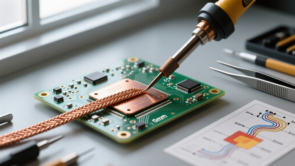
This method utilizes pre-cut copper shapes (dots or pads) backed with a thermosetting acrylic or polyimide (Kapton) adhesive. The new copper pad is aligned over the damaged area, bonded with heat or UV light, and then soldered to the remaining trace.
Technique & Specifications
- Material: 1 oz or 2 oz copper foil dots with polyimide backing (e.g., CircuitWorks replacement pad kits).
- Bonding Process: The adhesive requires a curing phase. Acrylic adhesives typically require a heat gun or hot plate at 120°C for 15 minutes, followed by an anaerobic catalyst or UV exposure depending on the specific product line.
- Soldering: Once cured, the pad is tinned with a low-temperature alloy like Sn42/Bi57/Ag1 (melting point 138°C) to prevent re-melting the adhesive bond during component attachment.
- Cost: $35 to $50 for a comprehensive replacement pad kit containing assorted sizes.
Pros & Cons
Pros: Restores the original visual geometry of the PCB. Excellent for high-pin-count surface-mount ICs where a wire jump would cause short circuits.
Cons: The Z-axis (vertical) tensile strength is entirely dependent on the adhesive bond. If subjected to heavy mechanical stress (e.g., plugging/unplugging a connector), the replacement pad can lift again.
Method 3: Conductive Silver Epoxy
Silver-filled conductive epoxies are used to rebuild a pad by painting the resin directly onto the exposed substrate and overlapping the surviving trace.
Technique & Specifications
- Material: Two-part silver conductive epoxy, such as MG Chemicals 8331 Silver Conductive Epoxy.
- Curing Profile: Standard cure is 24 hours at 25°C. For accelerated production, it can be heat-cured at 80°C for 15 minutes.
- Electrical Specs: Volume resistivity is typically around 0.0006 Ω·cm. While conductive, it is orders of magnitude higher resistance than pure copper.
- Cost: $60 to $85 per 14-gram dual-chamber syringe.
Pros & Cons
Pros: Extremely easy to apply in tight spaces without a soldering iron. Ideal for flexible PCBs (flex circuits) and heat-sensitive substrates that cannot tolerate thermal soldering.
Cons: Susceptible to silver migration in high-humidity environments if a DC bias is present, which can cause latent short circuits. Furthermore, the mechanical shear strength is significantly lower than soldered copper.
Comparison Matrix: Choosing the Right Method
| Feature | Wire Jumping | Copper Dots/Tape | Silver Epoxy |
|---|---|---|---|
| Tensile Strength | Excellent (Metallurgical bond) | Moderate (Adhesive dependent) | Poor to Moderate |
| Electrical Resistance | Negligible (~0.03 Ω) | Very Low (~0.05 Ω) | Low/Moderate (~2-5 Ω) |
| Thermal Tolerance | High (>200°C) | Moderate (~120°C limit) | Moderate (~150°C limit) |
| Aesthetics | Poor (Visible wire) | Excellent (Looks OEM) | Good (Painted look) |
| Best Application | Through-hole, heavy connectors | QFP, SOIC, SMD IC pads | Flex PCBs, RFID, low-current |
Step-by-Step: Executing a Reliable Wire Jump Repair
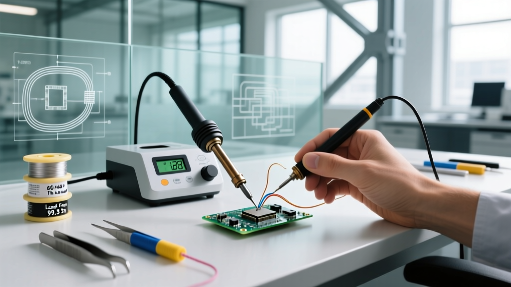
For high-reliability repair pad soldering work, the wire jump remains the gold standard. Follow this procedure to ensure IPC-compliant results:
- Trace Preparation: Use a fiberglass scratch pen to gently remove the solder mask and expose the copper trace leading away from the damaged pad. Clean with 99% isopropyl alcohol (IPA).
- Wire Stripping: Cut a length of 30 AWG Kynar wire. Use thermal strippers to remove exactly 2mm of insulation from both ends. Thermal strippers prevent nicking the copper core, which creates stress risers.
- Tinning: Apply a microscopic amount of no-clean flux (e.g., Amtech NC-559-V2-TF) to the exposed trace and the wire tips. Tin both surfaces with a 0.5mm chisel tip iron at 330°C.
- Soldering the Joint: Position the wire onto the exposed trace using precision tweezers. Apply the iron for 1.5 seconds to reflow the joint. The solder should wick smoothly, forming a concave fillet.
- Routing and Securing: Route the wire to the component lead or via. Solder the destination joint. Trim excess wire flush with the joint using flush cutters.
- Encapsulation: Apply a drop of UV-curable solder mask resin (e.g., Senju O-UM2000) over the exposed wire and the original damaged pad area. Cure under a 365nm UV lamp for 3 minutes to lock the wire in place and prevent mechanical fatigue.
Frequently Asked Questions
Can I just use superglue (cyanoacrylate) to reattach a lifted pad?
No. Standard cyanoacrylate (CA) is non-conductive and lacks the thermal stability required for PCB environments. While it might physically hold a pad in place, it will not restore electrical continuity, and it will outgas and degrade when exposed to the heat of subsequent soldering processes.
How do I prevent pad cratering during future rework?
Pad cratering (where the pad lifts and takes a chunk of the underlying fiberglass laminate with it) is caused by mechanical force on a cold joint. Always ensure the solder is fully molten (liquidus state) before applying any extraction force. Utilizing pre-heaters set to 130°C reduces the thermal delta required by the top-side iron, minimizing localized thermal shock to the FR4 substrate.
Is silver epoxy safe for high-frequency RF boards?
Generally, no. The silver particles in conductive epoxies create microscopic parasitic capacitances and inductances that can disrupt impedance-controlled RF traces (like 50-ohm microstrip lines). For RF repair pad soldering work, precision copper tape with high-frequency laminates (like Rogers RO4003C) is the required approach.