
The Physics of Wetting: Why Temperature Dictates Reliability
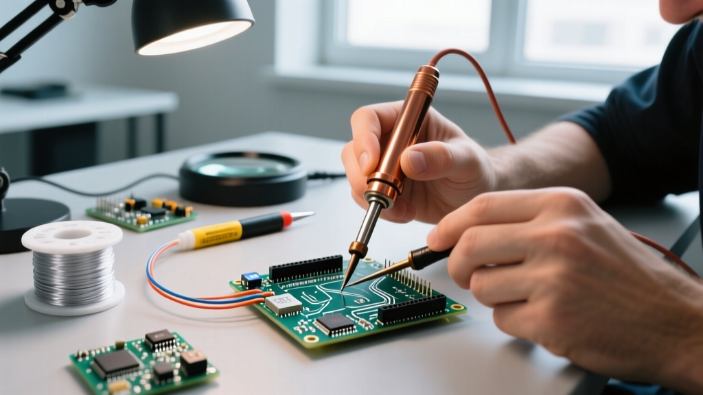
In high-volume electronics manufacturing and advanced prototyping, determining the correct soldering temp for circuit boards is not a matter of guesswork; it is a strict thermodynamic calculation. The reliability of an electronic assembly hinges on the formation of a precise intermetallic compound (IMC) layer between the component lead, the solder alloy, and the copper pad. If the thermal energy applied is insufficient, the solder will fail to wet the surfaces, resulting in a high-resistance mechanical bond. If the thermal energy is excessive, it accelerates IMC overgrowth, leading to brittle joints, and risks delaminating the printed circuit board (PCB) substrate.
For process engineers and advanced DIY practitioners operating in 2026, understanding the delta between the soldering iron's tip temperature and the actual wetting temperature at the pad interface is critical. The thermal mass of the component, the copper weight of the PCB (e.g., 1 oz vs. 3 oz), and the presence of internal ground planes all act as heat sinks, rapidly drawing thermal energy away from the joint. Therefore, the optimal soldering temp for circuit boards must account for both the alloy's liquidus point and the thermal recovery rate of the equipment being used.
Industry-Standard Soldering Temp for Circuit Boards: Alloy Matrix
Different solder alloys require vastly different thermal profiles. The transition from legacy leaded solders to RoHS-compliant lead-free alloys fundamentally shifted the thermal requirements in the electronics manufacturing industry. Below is a comprehensive matrix detailing the target parameters for the most common industrial alloys.
| Alloy Designation | Composition | Liquidus Temp | Target Iron Tip Temp | Max Dwell Time | Primary Application |
|---|---|---|---|---|---|
| SN63PB37 | 63% Sn / 37% Pb | 183°C (361°F) | 300°C - 320°C | 3 - 5 seconds | Aerospace, Medical, Legacy Repair |
| SAC305 | 96.5% Sn / 3% Ag / 0.5% Cu | 217°C (423°F) | 340°C - 360°C | 2 - 4 seconds | Consumer Electronics, Automotive, IoT |
| SAC405 | 95.5% Sn / 4% Ag / 0.5% Cu | 217°C (423°F) | 345°C - 365°C | 2 - 4 seconds | High-Reliability Industrial Controls |
| SN42BI58 | 42% Sn / 58% Bi | 138°C (280°F) | 200°C - 230°C | 3 - 5 seconds | Thermally Sensitive Components, LEDs |
| SN96.5AG3.0CU0.5 (Low-Ag) | SAC305 Variant | 217°C (423°F) | 350°C - 370°C | 2 - 4 seconds | High-Density Interconnect (HDI) Boards |
Note: Target iron tip temperatures assume a high-quality, temperature-sensing station with rapid thermal recovery. When soldering to heavy ground planes, tip temperature may need to be increased by 15°C to 20°C to compensate for instantaneous heat dissipation.
IPC and NASA Thermal Excursion Limits
In industrial applications, adherence to established quality standards is non-negotiable. According to the IPC J-STD-001 standard for soldered electrical and electronic assemblies, the thermal excursion of components must be strictly controlled to prevent internal damage to semiconductor dies and passive element terminations. The standard dictates that the maximum temperature and time a component can endure is defined by the component manufacturer's datasheet, but generally, a peak temperature of 260°C should not be exceeded for more than 10 seconds on the component body.
Furthermore, guidelines published by the NASA Electronic Parts and Packaging (NEPP) Program emphasize the dangers of thermal shock during manual touch-up and rework. NASA workmanship standards mandate that operators must never apply a cold soldering iron directly to a joint and ramp the temperature up slowly. The iron must be pre-heated to the correct soldering temp for circuit boards before making contact, ensuring the joint reaches reflow temperature in under three seconds. Prolonged application of a low-temperature iron causes heat to conduct up the component lead into the silicon die, potentially causing catastrophic latent failures that bypass initial quality control testing.
Process Engineer's Callout: Never rely on the digital readout of a budget soldering station as the absolute truth at the wetting interface. A station may read 350°C, but if the tip is heavily oxidized or the heater cartridge lacks the wattage to overcome a 4-layer PCB's thermal mass, the actual temperature at the copper pad may drop below the 217°C liquidus threshold of SAC305, resulting in a disturbed grain structure.
Failure Mode Analysis: The Cost of Thermal Mismanagement
Deviating from the optimal soldering temp for circuit boards introduces specific, documented failure modes that compromise the long-term reliability of the assembly.
Overheating: IMC Overgrowth and Substrate Damage
When the soldering temperature exceeds 380°C for SAC alloys, or when dwell times extend beyond 5 seconds, the copper-tin intermetallic layer grows disproportionately thick. A healthy IMC layer (primarily Cu6Sn5) should be between 1 to 3 micrometers thick. Excessive heat drives the formation of the Cu3Sn phase and introduces Kirkendall voids—microscopic gaps within the IMC layer that act as stress concentrators. Under mechanical or thermal cycling, these joints will fracture. Additionally, excessive tip temperatures degrade the PCB's FR-4 substrate, leading to pad lifting, barrel cracking in plated through-holes (PTH), and the charring of flux residues, which can create parasitic leakage paths in high-impedance circuits.
Underheating: Cold Joints and Dewetting
Conversely, applying insufficient heat prevents the flux chemistry from fully activating. Modern no-clean fluxes (classified as ROL0 or ROL1 per IPC J-STD-004) require specific activation temperatures—typically between 150°C and 180°C—to effectively strip oxides from the copper pads. If the soldering temp for circuit boards is too low, the flux remains inert, and the molten solder will ball up and dewet from the pad. This results in a 'cold joint,' characterized by a dull, gray, and grainy appearance. Cold joints possess high electrical resistance and lack mechanical strength, often failing during the very first power-on thermal expansion cycle.
Equipment Selection for High-Volume Thermal Recovery
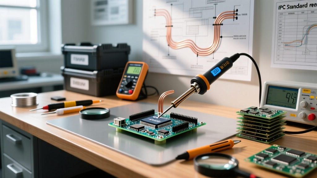
Achieving the correct soldering temp for circuit boards in an industrial environment requires equipment that utilizes closed-loop thermal feedback. Legacy analog stations are insufficient for modern lead-free profiles.
- Induction Heating Systems: Stations like the Hakko FX-951 utilize high-frequency induction to heat the tip directly. This eliminates the thermal lag inherent in traditional ceramic heater cartridges, allowing the tip to recover its target temperature in milliseconds after touching a heavy ground plane.
- High-Wattage Smart Stations: Systems like the Weller WX2021 (150W per channel) provide the raw thermal reserves necessary to maintain a stable 350°C tip temperature even when soldering large D-Pak connectors or multi-layer automotive ECUs.
- Tip Geometry Selection: Temperature is useless without efficient thermal transfer. Conical tips (e.g., B-type) have a microscopic contact area and are thermally starved. Process engineers must mandate the use of bevel or chisel tips (e.g., D-type or C-type) that match the width of the pad, maximizing the surface area for conductive heat transfer.
Thermal Profiling: Manual Touch-Up vs. Automated Reflow
It is vital to distinguish between the thermal profile of an automated reflow oven and manual hand soldering. In an automated reflow process, the entire PCB is subjected to a controlled ramp-soak-spike profile, where the entire board reaches thermal equilibrium before the peak reflow zone. In manual hand soldering, the thermal gradient is extreme: the tip is at 350°C, the solder joint reaches 230°C, and the adjacent component body may only reach 80°C. Because of this localized heating, the operator must actively manage the heat path by feeding solder wire directly into the iron-to-pad interface, using the melting solder as a liquid thermal bridge to transfer heat evenly into the component lead and the PCB pad simultaneously.
Summary Checklist for Process Engineers
To ensure optimal yield and reliability on the manufacturing floor, implement the following validation steps for your manual soldering operations:
- Verify Alloy Match: Confirm the solder wire alloy matches the PCB surface finish (e.g., use SAC305 for ENIG, SN63PB37 for HASL if exempt from RoHS).
- Calibrate Tip Thermocouples: Use a digital tip thermometer (e.g., Hakko FG-100B) to verify the actual tip temperature weekly, ensuring it is within ±5°C of the station's display.
- Audit Dwell Times: Conduct time-studies on operators. Any joint requiring more than 4 seconds of continuous iron contact indicates either an undersized tip, insufficient station wattage, or an incorrect temperature setting.
- Monitor Flux Activation: Ensure operators are not applying flux too early. Flux should be introduced just as the joint approaches the liquidus temperature to prevent premature burn-off.
Mastering the ideal soldering temp for circuit boards is the cornerstone of electronic assembly reliability. By respecting the thermodynamics of the alloys, adhering to IPC and NASA limits, and equipping operators with high-recovery tools, manufacturers can drastically reduce field failures and rework costs.