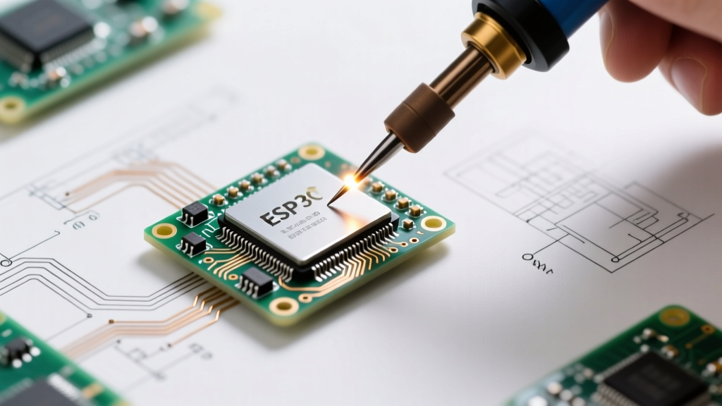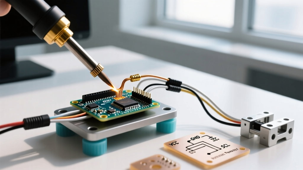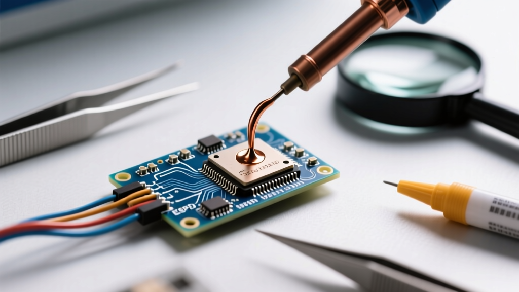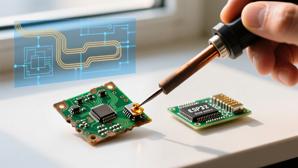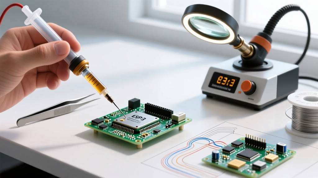

The Evolution of SMT SMD Soldering in Modern Electronics
Surface Mount Technology (SMT) and Surface Mount Devices (SMD) have entirely eclipsed traditional through-hole technology in modern electronics manufacturing. Whether you are prototyping a high-density IoT sensor board or repairing a multi-layer motherboard, mastering SMT SMD soldering is no longer optional for serious DIYers and electrical engineers. Unlike through-hole components that rely on mechanical leads passing through plated holes, SMDs sit flat on surface pads, demanding absolute precision in thermal management, paste application, and component alignment.
As we navigate the 2026 electronics landscape, component miniaturization has pushed standard sizes down to 0402 (1005 metric) and even 0201 imperial. These microscopic footprints leave zero margin for error. A slight over-application of solder paste or a two-second delay in thermal equilibrium can result in tombstoning, bridging, or latent cold solder joints. This comprehensive buyer's guide and technical manual will equip you with the exact tools, chemical profiles, and procedural frameworks required to execute flawless SMT SMD soldering in a home or small-batch lab environment.
Essential SMT SMD Soldering Equipment Buyer's Guide
Outfitting a lab for SMD work requires moving beyond basic 60W irons. You need rapid thermal recovery, precise airflow control, and micro-soldering tips. Below is a comparison of the industry-standard stations currently dominating the advanced DIY and professional rework space.
| Equipment Model | Category | Avg. Price (2026) | Temp Range | Best Application |
|---|---|---|---|---|
| Quick 861DW | Hot Air Rework | $260 - $280 | 100°C - 500°C | QFN/BGA reflow, multi-pin IC removal |
| Hakko FX-951 | Soldering Station | $350 - $380 | 200°C - 450°C | Drag soldering, precision touch-ups |
| JBC CD-2BQE | Premium Station | $550 - $600 | 150°C - 450°C | Ultra-fast recovery for heavy ground planes |
| Pine64 Pinecil V2 | Portable Iron | $26 - $30 | 100°C - 450°C | Budget field repairs, basic 0805 SMDs |
Buyer's Insight: If you are strictly working with 0805 and SOIC-8 packages, a high-quality iron like the Hakko FX-951 with a micro-pencil tip (e.g., B2 tip) is sufficient. However, once you transition to QFN (Quad Flat No-leads) or BGA (Ball Grid Array) packages, a hot air station like the Quick 861DW becomes mandatory. The 861DW's brushless fan provides the stable, low-vibration airflow necessary to reflow dense ICs without blowing adjacent 0402 capacitors off the board.
Solder Paste, Flux, and Stencil Chemistry
The chemical backbone of SMT SMD soldering is solder paste—a thixotropic mixture of microscopic solder spheres and tacky flux. Choosing the right paste and stencil thickness is where most beginners fail.
Understanding Paste Types and Alloys
Solder pastes are categorized by the IPC (Institute for Printed Circuits) based on the size of the solder spheres. According to the IPC standard J-STD-005, Type 3 paste (25-45 microns) is ideal for standard 0805 and 0603 components. However, for 0402 components and fine-pitch QFPs (0.5mm pitch), you must upgrade to Type 4 paste (20-38 microns) to prevent bridging and ensure smooth stencil release.
Pro Tip: For lead-free prototyping, SAC305 (Sn96.5/Ag3.0/Cu0.5) is the 2026 industry standard. It has a liquidus temperature of 217°C, requiring a peak reflow temperature of roughly 245°C. If you are not bound by RoHS compliance, Sn63/Pb37 (eutectic) melts at a much lower 183°C, vastly reducing thermal stress on sensitive components and making manual hot-air reflow significantly more forgiving.
Stencil Thickness Matrices
When ordering laser-cut stainless steel stencils, thickness dictates paste volume. Using a 5-mil (0.127mm) stencil on a board with 0402 components and 0.5mm pitch ICs will guarantee solder bridging. Follow this matrix for optimal paste deposition:
- 4 mil (0.10mm): Mandatory for 0402, 0201, and fine-pitch QFN/BGA pads.
- 5 mil (0.127mm): Standard for 0805, 0603, SOIC, and standard QFPs.
- 6 mil (0.152mm): Reserved for large power pads, D-PAK, and heavy through-hole pin-in-paste applications.
Step-by-Step Manual SMT Reflow Process
While automated pick-and-place machines handle high-volume manufacturing, manual SMT SMD soldering using a hot air gun and solder paste is the standard for prototyping. Follow this exact thermal profile to mimic a professional reflow oven.
- Stencil Alignment and Paste Application: Secure the PCB and stencil using high-temperature Kapton tape. Apply a bead of Type 4 SAC305 paste across the top of the stencil apertures. Using a rigid metal squeegee held at a strict 45-degree angle, pull the paste across the stencil with firm, even pressure. Peel the stencil straight up to avoid smearing.
- Component Placement: Using ESD-safe carbon fiber tweezers (such as the Vetus ST-15), place components into the wet paste. The tackiness of the flux will hold them in place. Do not press down hard; the paste should displace slightly around the edges of the pads.
- Pre-Heating (Crucial Step): Never blast a room-temperature board with 350°C air. Use a PCB preheater set to 120°C for 3 minutes, or use your hot air station at 150°C from a 10cm distance to slowly bring the entire board up to the flux activation temperature. This prevents thermal shock and warping.
- Reflow Phase: Set your hot air station (e.g., Quick 861DW) to 350°C with an airflow setting of 30-40%. Hold the nozzle 3 to 4 cm above the target IC. Use a continuous, slow circular motion to heat the component and surrounding ground planes evenly. Watch for the paste to transition from a dull, grainy grey to a shiny, liquid silver. This phase transition (wetting) should take roughly 10 to 15 seconds per IC.
- Cooling and Inspection: Remove the heat immediately once the solder shines. Allow the board to cool naturally to room temperature. Do not blow on it or use compressed air, as rapid cooling can induce micro-cracks in the solder joints. Inspect under a 10x to 40x stereo microscope for proper fillet formation.
Troubleshooting Common SMD Defects
Even with perfect technique, environmental factors and material degradation can introduce defects. The NASA Electronic Parts and Packaging (NEPP) Program provides extensive documentation on solder workmanship and failure analysis. Below are the most common SMT defects and their precise remedies.
| Defect Name | Visual Symptom | Root Cause | Actionable Solution |
|---|---|---|---|
| Tombstoning | Component stands vertically on one end. | Uneven heating causing one pad to reflow before the other, pulling the component via surface tension. | Ensure symmetrical trace routing to ground planes. Pre-heat the board thoroughly before localized hot air application. |
| Solder Bridging | Short circuit between adjacent IC pins. | Excessive paste volume, incorrect stencil thickness, or insufficient flux activation. | Reduce stencil thickness to 4 mil. Apply additional liquid no-clean flux before rework to improve surface tension. |
| Cold Solder Joint | Dull, grainy, or cracked joint appearance. | Insufficient peak temperature or inadequate time above liquidus (TAL). | Increase hot air temperature by 15°C or extend dwell time. Verify ground planes are not acting as massive heat sinks. |
| Solder Balling | Microscopic spheres of solder scattered on the mask. | Moisture in the solder paste or rapid outgassing of volatile flux compounds. | Store solder paste in a refrigerator and allow it to reach room temperature before opening. Extend the pre-heat phase. |
Advanced Upgrades: Reflow Ovens and AOI
As your production scales from single prototypes to batches of 50+ boards, manual hot air reflow becomes a bottleneck. Upgrading to a benchtop reflow oven (such as the NeoDen 4 or a modified toaster oven with a PID controller) ensures strict adherence to the J-STD-020 reflow profile. Furthermore, integrating Automated Optical Inspection (AOI) or utilizing high-resolution USB microscopes with measurement software allows you to catch bridging and misalignment before the boards leave your lab.
Industry data and technical discussions frequently highlighted on portals like CircuitNet emphasize that the transition from manual SMD soldering to automated batch reflow reduces defect rates by over 85%, primarily by eliminating the human variable in thermal management.
Frequently Asked Questions (FAQ)
Can I use a standard soldering iron for SMT SMD soldering without paste?
Yes, but it requires a different technique known as 'drag soldering' or 'tack-and-solder.' You must first tin one pad, tack the component in place with tweezers, and then apply liquid flux and drag a heavily tinned micro-tip across the remaining pins. While viable for SOIC and TSSOP packages, this method is virtually impossible for QFN or BGA components where the pads are hidden beneath the chip body.
How long does solder paste last once opened?
Unopened, refrigerated solder paste typically has a shelf life of 6 to 12 months. Once opened and exposed to ambient humidity and temperature, its efficacy degrades rapidly. For optimal results, use opened paste within 2 to 4 weeks. If the paste begins to separate or loses its tackiness, discard it; attempting to reflow degraded paste will result in severe solder balling and cold joints.
What is the best way to clean no-clean flux residues?
While 'no-clean' flux is designed to be left on the board, it can sometimes leave a sticky or cosmetically unappealing residue. To clean it, use a high-quality PCB cleaner like Chemtronics Electro-Wash or pure isopropyl alcohol (99%+ IPA). Apply the solvent, gently agitate with an ESD-safe boar-bristle brush, and immediately wipe away the dissolved flux with a lint-free Kimwipe before the solvent evaporates and re-deposits the sticky flux resins back onto the board.