
The Stakes of High-Reliability Soldering in 2026
In the consumer electronics space, a marginal solder joint might result in a returned smartphone and a minor warranty claim. In aerospace, medical, and automotive applications, that same joint can lead to catastrophic system failure, loss of life, and millions in liability. As surface-mount components shrink to 01005 (0.4mm x 0.2mm) and BGA pitch sizes drop below 0.35mm, executing a proper soldering technique is no longer just about making an electrical connection; it is about engineering a metallurgical bond that survives extreme thermal cycling, vibration, and humidity.
For industry professionals and advanced DIY engineers building mission-critical hardware, understanding the physics of wetting, intermetallic compound (IMC) formation, and flux chemistry is mandatory. This guide breaks down the exact parameters required to meet IPC-A-610 Class 3 and J-STD-001 standards, moving beyond basic tutorials into the applied science of high-reliability electronics manufacturing.
Decoding IPC J-STD-001: What Defines a 'Proper' Joint?
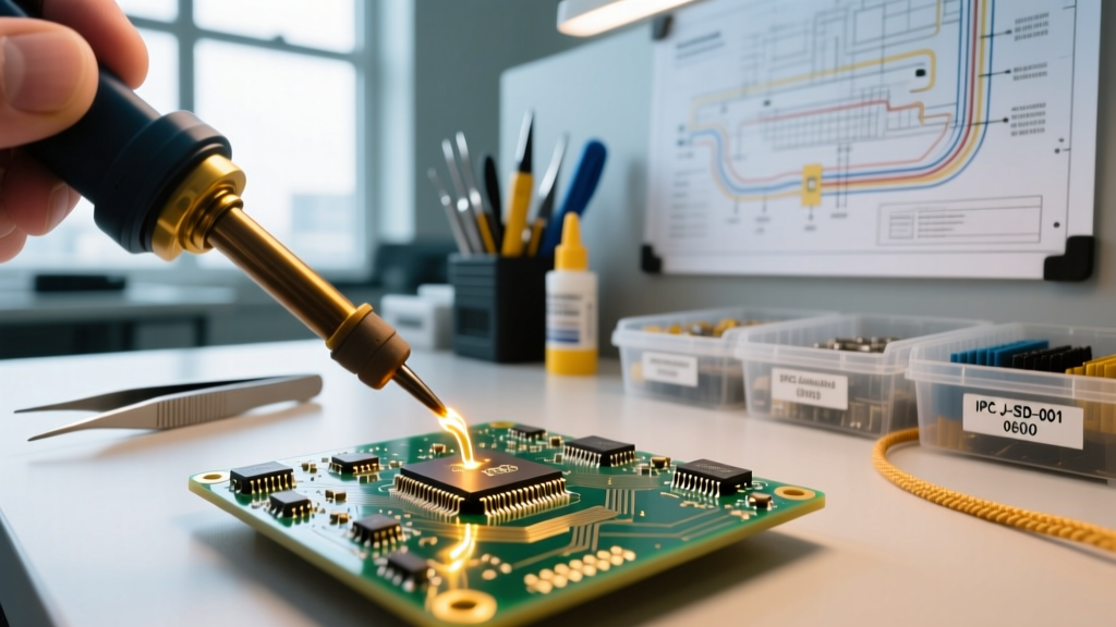
The IPC J-STD-001 standard dictates the requirements for soldered electrical and electronic assemblies. When engineers refer to a proper soldering technique in an industrial context, they are usually referring to achieving Class 3 (High-Reliability) target conditions. Unlike Class 1 (General Electronic Products) where the primary goal is simple functionality, Class 3 demands that the joint maintains structural integrity under severe environmental stress.
Target vs. Acceptable vs. Defect
- Target Condition: The ideal scenario. For through-hole components, this means 100% barrel fill (though 75% is the minimum acceptable for Class 3 with specific design allowances), a smooth, concave fillet, and a wetting angle of less than 90 degrees (ideally 15 to 30 degrees).
- Acceptable Condition: The joint may lack perfect aesthetics but meets minimum electrical and mechanical requirements. The solder fillet might be slightly convex, but wetting is evident on both the pad and the lead.
- Defect: Non-wetting, cold joints, disturbed joints, or excessive solder (which can hide the underlying pad geometry and mask a lack of wetting). In Class 3, a disturbed joint during the cooling phase is an automatic failure.
According to the IPC Standards Documentation, achieving these target conditions relies entirely on thermal equilibrium and correct flux activation, not merely melting solder onto a pad.
Thermal Profiling: The Core of Proper Soldering Technique
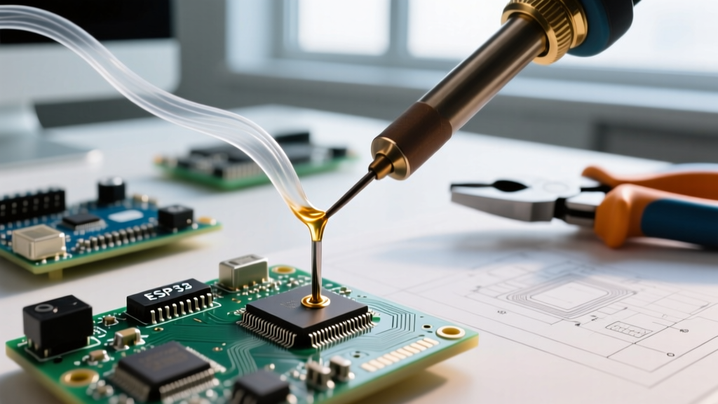
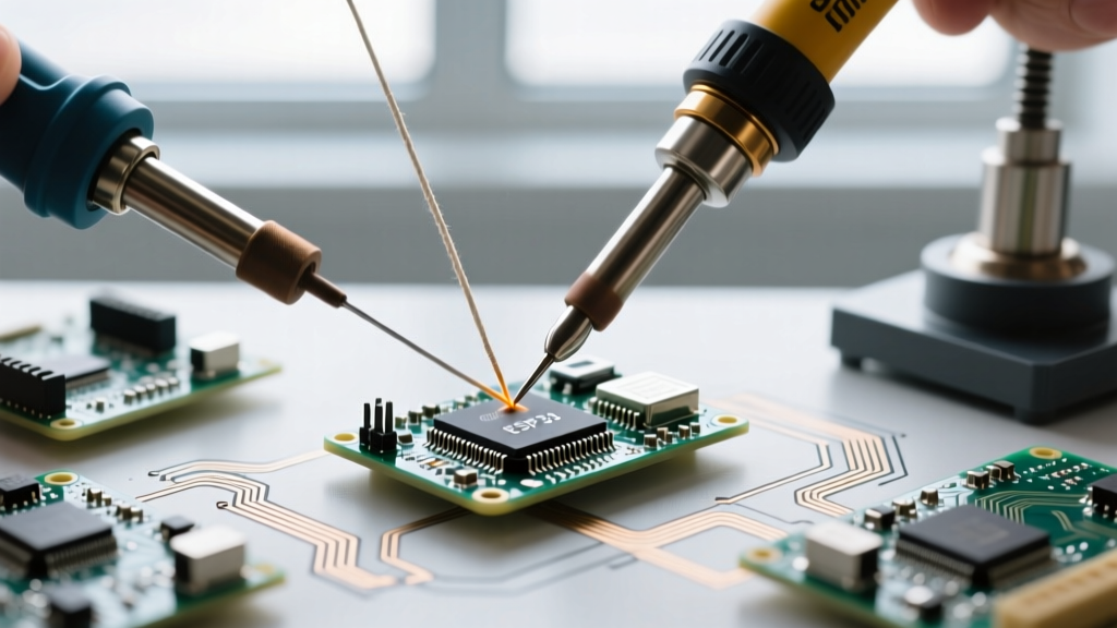
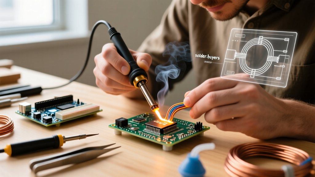
The most common failure in manual and automated soldering is improper thermal profiling. A proper soldering technique requires the simultaneous heating of the component lead and the PCB pad to a temperature slightly above the solder alloy's liquidus point before the solder wire is introduced.
Industry Solder Alloy Matrix
| Alloy Composition | Melting Point | Optimal Tip Temp | Max Dwell Time | Primary Industry Application |
|---|---|---|---|---|
| Sn63Pb37 (Leaded) | 183°C (Eutectic) | 320°C - 340°C | 2.0 - 3.0 seconds | Aerospace, Military (Legacy/Exempt) |
| SAC305 (Lead-Free) | 217°C - 220°C | 350°C - 370°C | 2.5 - 4.0 seconds | Automotive, Medical, Commercial |
| Sn96.5/Ag3.0/Cu0.5 | 217°C | 350°C - 365°C | 2.0 - 3.5 seconds | High-Vibration Industrial |
| In100 (Pure Indium) | 157°C | 240°C - 260°C | 1.0 - 2.0 seconds | Cryogenics, Thermal Interfaces |
Data sourced from standard metallurgical profiles and Indium Corporation Solder Alloy Guides.
When working with SAC305 (the industry standard lead-free alloy), the higher melting point requires more thermal energy. If your soldering iron lacks the thermal mass or recovery speed to maintain 360°C at the tip when it touches a heavy copper ground plane, the solder will cool prematurely, resulting in a grainy, disturbed joint. This is why high-end cartridge-based stations are mandatory for Class 3 work.
Flux Selection and Chemistry for Mission-Critical Boards
Flux is arguably more important than the solder itself. A proper soldering technique is impossible without the correct flux chemistry to remove metal oxides and lower the surface tension of the molten alloy. Under IPC J-STD-004, fluxes are categorized by material, activity level, and halide content.
Industrial Flux Classifications
- ROL0 (Rosin, Low Activity, 0% Halides): The gold standard for medical and aerospace hardware. It is highly reliable, leaves a benign, non-conductive residue, and does not require cleaning. However, it struggles to wet heavily oxidized pads.
- ROL1 (Rosin, Low Activity, Halides present): Better wetting than ROL0, but the halide content can cause long-term electrochemical migration (dendritic growth) in high-humidity environments if not cleaned.
- ORH0 (Organic, High Activity, 0% Halides): Used for difficult-to-solder surfaces like nickel-palladium-gold (NiPdAu) finishes. Mandatory cleaning is required post-soldering, as organic acid residues are highly corrosive and conductive.
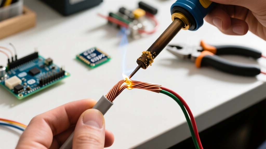
According to the NASA Workmanship Training Program, flux application must precede the heat source. Applying solder directly to the iron tip and attempting to transfer the molten blob to the joint burns off the flux before it can clean the substrate, resulting in a classic 'cold joint' defect.
Edge Cases and Failure Modes: The IMC Layer
Every time you execute a proper soldering technique, an Intermetallic Compound (IMC) layer forms between the copper pad and the tin in the solder. For SAC305 and copper, this forms Cu6Sn5 and Cu3Sn phases. This layer is what actually bonds the joint; without it, you just have solder sitting on top of copper.
The Danger of Overheating
The ideal IMC layer thickness is between 1.0 and 2.0 microns. If the dwell time exceeds 4 seconds, or if the tip temperature is set too high (e.g., >400°C for SAC305), the IMC layer can grow to 5 microns or more. While a thicker IMC layer might sound stronger, it is actually highly brittle. In automotive under-hood applications subject to thermal shock (-40°C to 125°C), a thick IMC layer will micro-fracture, leading to intermittent resistance spikes and eventual open-circuit failure.
Conversely, if the temperature is too low or the dwell time is under 1 second, the IMC layer may not form completely, resulting in a non-wetting condition where the solder beads up and separates from the pad under minor mechanical stress.
Essential Tooling for Industry-Grade Results
You cannot achieve IPC Class 3 targets with a $30 variable-temperature iron. The tooling must feature rapid thermal recovery and precise tip-to-sensor geometry.
- JBC CD-2BQE with T245 Handle (~$475): JBC's cartridge system places the heating element and thermocouple inside the tip itself. When a T245 tip hits a massive copper pour, it detects the temperature drop and recovers to 360°C in under 0.8 seconds, preventing the operator from lingering and overheating the pad.
- Weller WX1 with WXMP Micro Pencil (~$650): Ideal for 0201 and 01005 components. The micro-pencil tips offer high precision, and the Weller heating element provides excellent steady-state temperature control, crucial for preventing tombstoning on micro-passives.
- Hakko FX-951 with T18 Series (~$285): The industry workhorse for general Class 2 and light Class 3 work. While slightly slower to recover than JBC, its composite ceramic heating element is highly durable and cost-effective for production environments.
Frequently Asked Questions
How do I prevent tombstoning on micro-passives?
Tombstoning occurs when one side of a component's solder paste melts before the other, and the wetting force pulls the component upright. A proper soldering technique for manual rework involves pre-heating the entire PCB to 100°C - 120°C on a hotplate before applying the iron, ensuring both pads reach the liquidus temperature simultaneously.
Is it acceptable to use liquid flux pens for aerospace rework?
Yes, but only if the flux chemistry matches the original assembly requirements (typically ROL0). Furthermore, the solvent in the pen must be allowed to flash off for 10-15 seconds before applying heat; otherwise, the rapid boiling of the solvent can cause solder spatter, creating micro-spheres that bridge adjacent fine-pitch leads.
What is the maximum time allowed to complete a single through-hole joint?
IPC guidelines generally recommend a maximum dwell time of 3 to 4 seconds. If the joint is not properly wetted within this window, you must remove the heat, allow the pad to cool to room temperature, and reassess your thermal profile or pad oxidation before attempting a second pass.