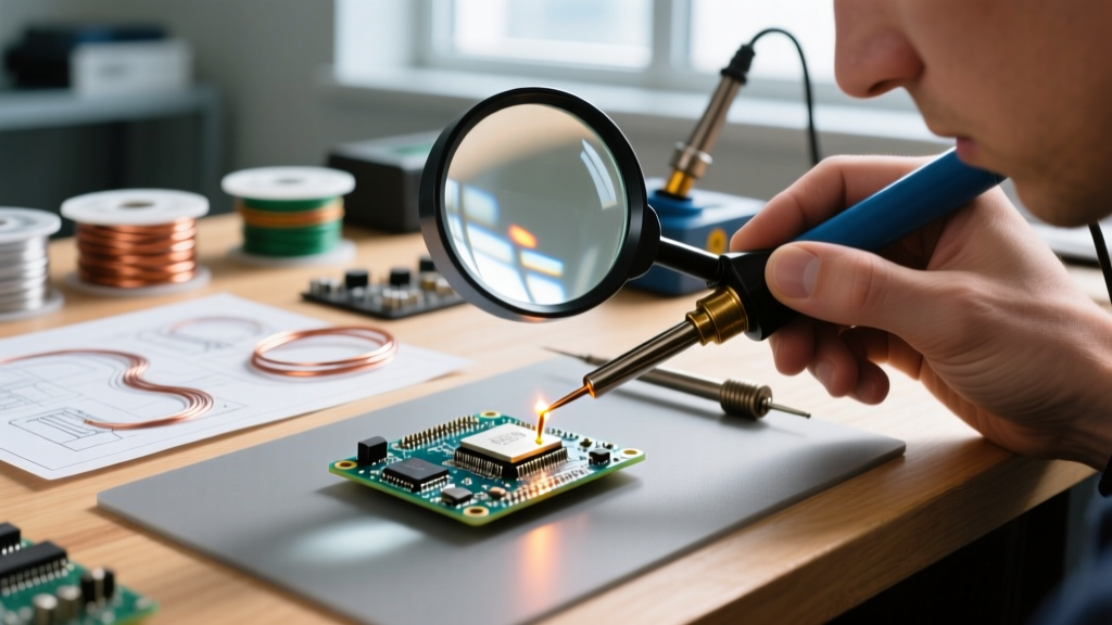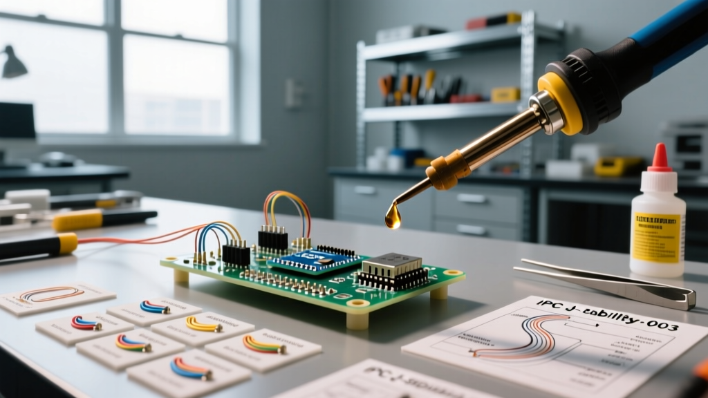

What is a Solderability Testing Service?
When prototype assemblies fail on the SMT line or wave soldering yields drop below 98%, the root cause often traces back to the metallurgical surface of the bare printed circuit board (PCB) or the component leads. A professional solderability testing service provides quantitative and qualitative analysis of how well a surface will accept molten solder. Rather than relying on visual inspection or trial-and-error on the assembly line, these specialized laboratories simulate the soldering process under strictly controlled conditions to identify oxidation, contamination, or plating defects before full-scale production begins.
For electronics manufacturers, hardware startups, and high-reliability DIYers building aerospace or medical devices, outsourcing this testing is a critical risk-mitigation step. The governing standard for bare boards is IPC J-STD-003 (Solderability Tests for Printed Boards), while component leads are tested under IPC J-STD-002. Understanding what these labs actually do—and when you need them—is essential for optimizing your 2026 manufacturing budget.
Core Testing Methods Explained
Reputable testing laboratories offer a tiered approach to solderability analysis. The method chosen depends on the board's surface finish, the component pitch, and the required reliability class (e.g., Class 2 for standard consumer electronics vs. Class 3 for aerospace/medical).
| Test Method | Best Application | Primary Metric | IPC Standard Reference |
|---|---|---|---|
| Dip and Look | Through-hole, large SMT pads, general PCB finishes | Visual % coverage (meniscus) | J-STD-003 Clause 4.1 |
| Surface Mount Test | Fine-pitch SMT pads, BGA footprints | Solder ball adhesion & wetting | J-STD-003 Clause 4.2 |
| Wetting Balance | Ultra-fine pitch, component leads, quantitative R&D | Wetting force (mN) & Time to zero | J-STD-002 / J-STD-003 |
| Solder Float | Thermal shock resistance of bare laminates | Delamination / blistering check | J-STD-003 Clause 4.4 |
1. Dip and Look (The Industry Workhorse)
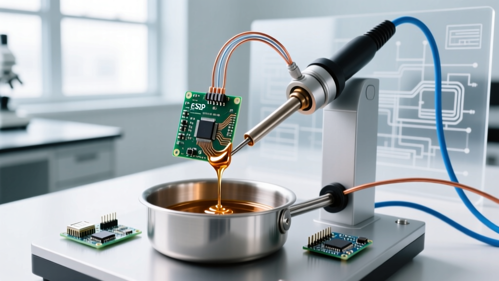
The 'Dip and Look' method is the most common qualitative test. The lab applies a standardized flux (typically Type ROL0 or ROL1 per IPC J-STD-004) to the test coupon or PCB edge. The sample is then immersed in a static solder pot. For legacy tin-lead (Sn63Pb37) processes, the pot is held at 245°C ± 5°C. For modern lead-free SAC305 (Tin-Silver-Copper) alloys, the temperature is raised to 255°C ± 5°C. After a 3 to 5-second dwell time, the board is extracted and inspected under magnification. For Class 2 products, a minimum of 95% continuous solder coverage is required; Class 3 demands near-perfect wetting with no exposed base metal or dewetting.
2. Wetting Balance Testing (Quantitative Precision)
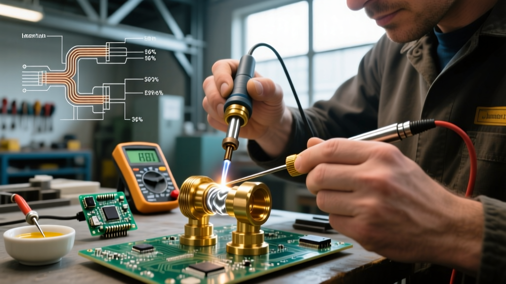
When visual inspection isn't enough—such as when evaluating 0.4mm pitch BGAs or investigating intermittent cold solder joints—labs use a meniscograph (wetting balance). This instrument measures the actual physical force (in millinewtons, mN) exerted by molten solder as it climbs the test specimen. The lab records the 'Time to Zero' (the exact millisecond the upward wetting force overcomes the downward buoyancy force) and the maximum wetting force. According to SMTA technical guidelines, a faster time-to-zero and a higher maximum force indicate superior solderability, providing hard data for R&D teams comparing different PCB fabricators.
3. Surface Mount Test (SMT Pad Specific)
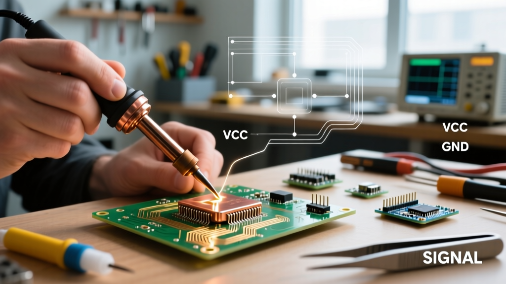
Designed specifically for surface mount pads, this test involves placing a standardized solder sphere (often 0.75mm or 1.0mm diameter) on a fluxed pad and applying heat via a hot plate or localized hot air. The test measures whether the solder sphere collapses and wets the pad uniformly within a specific timeframe, simulating reflow oven conditions without risking the entire board.
The Crucial Role of Accelerated Aging
Testing a PCB straight from the manufacturer's vacuum-sealed bag only tells you if it is solderable today. To simulate warehouse shelf life, a professional solderability testing service will perform accelerated aging before the solder dip.
Expert Insight: The industry standard for accelerated aging is steam aging. Exposing the PCB to 100°C steam for 8 hours in a specialized autoclave simulates approximately 6 to 12 months of ambient warehouse storage. If a board passes the Dip and Look test after 8 hours of steam aging, you can confidently approve the lot for long-term production runs.
Alternatively, dry heat aging (e.g., 155°C for 16 hours) is sometimes used for high-temperature polyimide flex circuits, though steam remains the benchmark for standard FR-4 rigid boards with OSP or ENIG finishes.
2026 Pricing and Turnaround Expectations
Budgeting for third-party lab services requires understanding the breakdown of costs. While prices vary by region and laboratory accreditation, the following table represents standard North American and European market rates for 2026.
| Service Tier | Includes | Estimated Cost (per lot/sample set) | Typical Turnaround |
|---|---|---|---|
| Basic Qualification | Dip & Look (as-received), 3 coupons | $200 - $350 | 3 - 5 Days |
| Standard Shelf-Life | 8-Hour Steam Aging + Dip & Look | $350 - $550 | 5 - 7 Days |
| Advanced Quantitative | Wetting Balance Testing (Meniscograph) | $500 - $850 | 7 - 10 Days |
| Component Lead Audit | J-STD-002 testing on IC/reel samples | $250 - $450 | 4 - 6 Days |
Common Failure Modes Identified by Labs
When a solderability test fails, the lab's failure analysis report will typically point to one of the following specific metallurgical breakdowns:
- ENIG Black Pad Syndrome: A catastrophic failure mode in Electroless Nickel Immersion Gold finishes where hyper-corrosion of the nickel layer creates a brittle, phosphorus-rich interface. Solder will initially wet, but the joint will fracture under minimal mechanical stress. Labs identify this via cross-section microscopy following a failed peel test.
- Immersion Silver Tarnishing: Silver is highly susceptible to sulfur and chlorine in the atmosphere. If the PCB fabricator failed to apply an adequate anti-tarnish organic inhibitor, the silver will form non-solderable sulfide layers. This is easily caught via the 8-hour steam aging test.
- OSP (Organic Solderability Preservative) Degradation: OSP is a thin organic layer that protects bare copper. If the board undergoes multiple unauthorized thermal excursions (like accidental baking to remove moisture) before assembly, the OSP breaks down, leading to severe oxidation and complete dewetting during the Dip and Look test.
- HASL Thinning on High Aspect Ratio Vias: Hot Air Solder Leveling can pull solder away from the edges of small vias due to surface tension and air knife pressure, leaving the base copper exposed and prone to rapid oxidation.
In-House Testing vs. Third-Party Laboratory
Many large EMS (Electronics Manufacturing Services) providers maintain an in-house solder pot and perform basic Dip and Look tests. However, relying on in-house testing has distinct limitations compared to hiring an independent service.
When to use In-House: Routine incoming inspection of high-volume, low-complexity consumer boards where a simple pass/fail visual check is sufficient. Note that maintaining a dedicated, uncontaminated static solder pot and calibrated thermocouples requires ongoing maintenance.
When to hire a Third-Party Service: You must hire an external lab when dealing with Class 3 aerospace/medical assemblies, when investigating a field failure or line-yield drop, or when qualifying a new, overseas PCB fabricator. Independent labs possess ISO/IEC 17025 accreditation, ensuring their measurement uncertainties, equipment calibrations, and environmental controls are audited by bodies like A2LA or UKAS. Furthermore, third-party labs have access to SEM/EDX (Scanning Electron Microscopy with Energy Dispersive X-ray Spectroscopy) to perform elemental analysis on failed pads—a capability rarely found on the standard factory floor.
How to Select the Right Testing Laboratory
Not all metallurgical labs specialize in electronics. When vetting a solderability testing service, use this checklist to ensure they meet modern industry requirements:
- Verify IPC Licensing: Ensure the lab is licensed to perform testing to the latest revision of IPC J-STD-003 and J-STD-002. Outdated revisions may not account for the thermal profiles of newer low-temperature alloys like SnBiAg.
- Check Alloy Capabilities: Confirm they have dedicated, segregated solder pots for both Sn63Pb37 (tin-lead) and SAC305/SAC405 (lead-free). Cross-contamination of lead into a RoHS-compliant lead-free pot will ruin your test validity and potentially contaminate your actual production line if samples are returned.
- Review Reporting Depth: A quality lab provides high-resolution micrographs, exact temperature logs of the solder pot during immersion, and specific references to the acceptance criteria tables within the IPC standard, rather than just a one-page 'Pass/Fail' certificate.
- Ask About NASA NEPP Alignment: For high-reliability projects, ask if their testing protocols align with NASA's Electronic Parts and Packaging Program guidelines, which often impose stricter wetting thresholds than standard commercial IPC Class 3.
Frequently Asked Questions
Can I test solderability on a fully assembled PCB?
No. Solderability testing (per J-STD-003) is designed for bare printed boards or unpopulated test coupons. If a board is already assembled and experiencing solder joint failures, you require a 'Solder Joint Reliability Analysis' or 'Cross-Sectional Failure Analysis' (often involving dye-and-pry tests or X-ray inspection), which is a completely different laboratory service.
How many test coupons should I send to the lab?
Standard practice requires a minimum of three test coupons per finish type to ensure statistical validity. Most PCB fabricators include 2 to 4 standardized solderability test coupons (usually featuring a mix of via barrels, SMT pads, and through-holes) on the production panel's breakaway rail. Always instruct your fab house to leave these coupons un-separated and include them in the shipment to the lab.
Does a passing solderability test guarantee good wave soldering results?
Not entirely. A passing test confirms the metallurgical surface is capable of wetting. However, wave soldering defects like bridging, icicles, or skipped joints are often caused by poor PCB layout (e.g., incorrect pad spacing, lack of solder thieves), improper flux application, or incorrect conveyor speed and preheat profiles on the assembly line. Solderability testing isolates the board finish variable from the assembly process variables.