
The Evolution of Desktop PCB Assembly Soldering
For hardware engineers, makers, and small-batch manufacturers, choosing the right PCB assembly soldering methodology is a critical bottleneck that dictates both yield and time-to-market. In 2026, the barrier to entry for professional-grade surface mount technology (SMT) has never been lower. Desktop reflow ovens and precision hotplates now compete directly with traditional hand soldering for prototyping runs of 10 to 50 boards. However, hand soldering remains indispensable for through-hole components, heavy mechanical connectors, and rapid design iterations.
This comprehensive buyer guide dissects the technical specifications, cost structures, and failure modes of hand versus reflow PCB assembly soldering, providing actionable frameworks to optimize your workbench.
Method 1: Precision Hand Soldering for SMD & Through-Hole
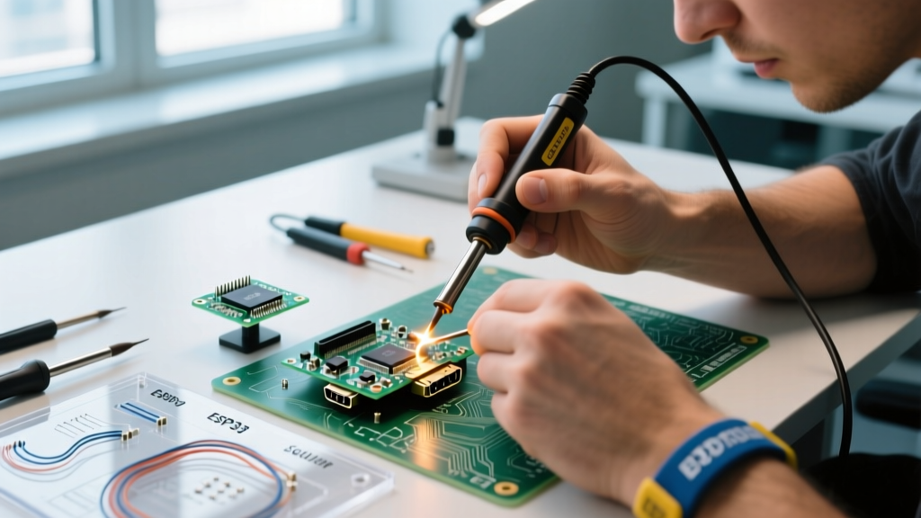
Hand soldering is often misunderstood as a purely manual, low-precision task. When executed with modern active-tip technology and correct metallurgy, it is highly capable of assembling fine-pitch SMD components down to 0402 packages and 0.5mm pitch QFPs.
Iron Selection & Active Tip Geometries
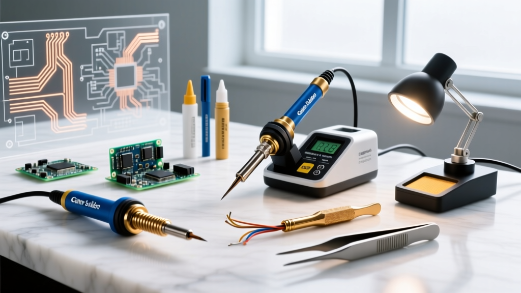
The industry standard for high-reliability hand PCB assembly soldering has shifted from traditional ceramic heating elements to active cartridge tips, where the heating element and thermocouple are integrated directly into the tip. This provides thermal recovery times measured in milliseconds.
- High-End Professional: The JBC CD-2BQF (approx. $580) paired with C245 series tips remains the benchmark. For drag-soldering fine-pitch QFPs, the C245-764 spoon tip holds a solder meniscus perfectly. For standard SOIC-8 and 0805 passives, the C245-945 2.2mm chisel provides optimal thermal transfer.
- Prosumer/Budget: The Weller WE1010NA (approx. $115) or the Pine64 Pinecil V2 (approx. $26) offer excellent value. While their thermal recovery is slower than JBC, they are perfectly adequate for 0603 passives and larger ICs.
Wire Solder Metallurgy: Eutectic vs. Lead-Free
For prototyping and non-RoHS restricted assemblies, Sn63Pb37 (63/37 Tin-Lead) remains the undisputed champion. It is a eutectic alloy, meaning it transitions directly from solid to liquid at a single temperature (183°C) without a plastic (paste) phase, drastically reducing cold-joint risks during minor hand movements.
When assembling for commercial deployment requiring RoHS compliance, SAC305 (Sn96.5/Ag3.0/Cu0.5) is the standard. It requires higher iron temperatures (350°C - 380°C) and exhibits a plastic phase between 217°C and 220°C, demanding a steadier hand to avoid disturbed joints.
Pro Tip: Always specify a 2.2% to 3.3% flux core by weight for hand PCB assembly soldering. No-clean wire solder (e.g., Kester 245) leaves a benign residue, while water-soluble cores require mandatory post-assembly cleaning to prevent dendritic growth.
Method 2: Reflow PCB Assembly Soldering for Batch Prototyping
When your bill of materials (BOM) exceeds 50 SMD components per board, or you are running a batch of 15+ identical PCBs, reflow soldering becomes exponentially more efficient. The process relies on depositing solder paste through a stencil, placing components, and heating the entire assembly through a controlled thermal profile.
Stencils and Paste Deposition
The foundation of a successful reflow process is the stencil. For mixed boards containing both 0402 passives and larger QFNs, a 4-mil (0.1mm) thick stainless steel stencil is optimal in 2026. Frameless foils (approx. $15-$25 from fabs like PCBWay or JLCPCB) require tensioning frames, while framed stencils ($80+) offer superior squeegee pressure consistency.
Solder paste selection is dictated by component pitch:
- Type 3 (25-45µm powder): Ideal for standard 0805, SOIC, and QFP components.
- Type 4 (20-38µm powder): Mandatory for 0402 passives, 0.4mm pitch BGAs, and micro-QFNs to prevent aperture clogging.
Paste must be stored at 0-10°C and allowed to acclimate to room temperature for at least 2 hours before opening to prevent moisture condensation, which causes severe solder spattering during reflow.
Thermal Profiling: The 4 Stages of Reflow
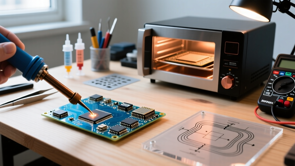
Whether using a $160 prosumer hotplate like the Miniware MHP50, a $2,500 desktop conveyor oven like the NeoDen YY1, or a DIY toaster oven modded with a PID controller, the thermal profile must adhere to the paste manufacturer's specifications. According to Indium Corporation Technical Resources, a standard Sn63Pb37 profile follows four distinct stages:
- Preheat (Ramp): 1°C to 2°C per second up to 150°C. Prevents thermal shock to ceramic capacitors.
- Soak (Dwell): 150°C to 180°C for 60-90 seconds. Activates the flux chemistry and volatizes solvents.
- Reflow (Peak): Ramp to a peak of 235°C. The Time Above Liquidus (TAL) — the time the paste spends above 183°C — must be strictly maintained between 45 and 60 seconds.
- Cooling: 2°C to 4°C per second. Rapid cooling ensures a fine grain structure in the solder joint, maximizing mechanical strength.
Cost, Yield, and Time Comparison Matrix
The following matrix compares the operational realities of different PCB assembly soldering setups for a hypothetical 50-board batch, each containing 40 SMD components and 5 through-hole connectors.
| Setup Method | Initial CapEx (2026) | Time Per Board (Batch) | Expected First-Pass Yield | Best Use Case |
|---|---|---|---|---|
| Hand Soldering (JBC Active) | $600 - $750 | 12 - 18 minutes | 85% - 92% | Prototypes, mixed THT/SMD, heavy connectors |
| Hotplate Reflow (MHP50) | $160 - $250 | 4 - 6 minutes | 75% - 85% | Single-sided SMD boards, ultra-low budget |
| Desktop Reflow Oven (NeoDen) | $2,500 - $8,000 | 45 seconds (conveyor) | 98% - 99.5% | Small-batch production, dense 0402/BGA boards |
Critical Defect Troubleshooting & Edge Cases
Even with optimized profiles, PCB assembly soldering introduces specific failure modes that require immediate diagnostic correction.
Tombstoning and Drawbridging
Tombstoning occurs when a passive component stands on one end during reflow. This is caused by uneven wetting forces, usually due to asymmetrical pad sizes, uneven stencil aperture reductions, or a component being placed slightly off-center. Fix: Implement a 10% home-plate aperture reduction in your stencil design for 0402 pads to balance surface tension.
Drawbridging (a specific type of shorting) happens when two adjacent pads pull solder toward each other, forming a bridge without a component. This is almost exclusively a result of excessive solder paste volume or a squeegee pressure that is too low during stencil printing.
Head-in-Pillow (HiP) and Solder Beading
Head-in-Pillow is a notorious defect in BGA and QFN assembly where the solder paste melts, but the component's solder ball oxidizes and fails to coalesce with the paste, resting on top like a head on a pillow. This is typically caused by insufficient peak temperature or warping of the BGA substrate. According to the NASA Electronic Parts and Packaging (NEPP) Program, verifying the Time Above Liquidus (TAL) with a physical thermocouple profile board is mandatory to eliminate HiP defects.
Solder Beading (small spheres of solder trapped under components) is caused by an aggressive ramp rate during the preheat stage, which boils the flux solvents before they can evaporate, splattering molten solder. Slowing the ramp rate to 1.5°C/sec resolves this.
Post-Assembly Cleaning and IPC Compliance
The decision to clean flux residue depends on the flux chemistry and the operational environment of the final product. While "no-clean" fluxes are designed to be left on the board, they can interfere with conformal coating adhesion and high-impedance analog circuits.
For water-soluble (OA) fluxes, cleaning is non-negotiable. The residue is highly corrosive and will cause electrochemical migration (dendrites) within weeks in humid environments. The IPC Standards for Electronics Assembly (specifically IPC-A-610) dictate strict cleanliness criteria for Class 2 and Class 3 aerospace/medical boards.
Recommended Cleaning Protocol:
- Solvent Cleaning: Use MG Chemicals 824-1L Isopropyl Alcohol (IPA) or specialized PCB wash for no-clean residues. Apply with an acid-free brush and immediately dry with compressed air to prevent dissolved flux from wicking under ICs.
- Ultrasonic Cleaning: For water-soluble fluxes, a 2L to 3L ultrasonic cleaner (e.g., VEVOR 2L, approx. $80) filled with a 5% saponifier solution (like Kyzen Aquanox) at 45°C for 6 minutes provides superior under-component cleaning. Warning: Do not use ultrasonic cleaning on boards containing MEMS sensors, unsealed potentiometers, or bare quartz crystals, as the cavitation can destroy micro-mechanical structures.
Final Verdict: Structuring Your Assembly Line
For the modern hardware lab in 2026, a hybrid approach to PCB assembly soldering is the most pragmatic. Invest in a high-quality active-tip hand soldering station (JBC or Weller) for through-hole components, connectors, and rapid single-board revisions. Simultaneously, utilize a desktop stencil printer and a mid-range reflow oven or high-precision hotplate for SMD-heavy batches. By matching the metallurgy, stencil aperture design, and thermal profile to the specific BOM requirements, you can achieve commercial-grade yields right on the workbench.