
The High-Stakes World of Motherboard Repair
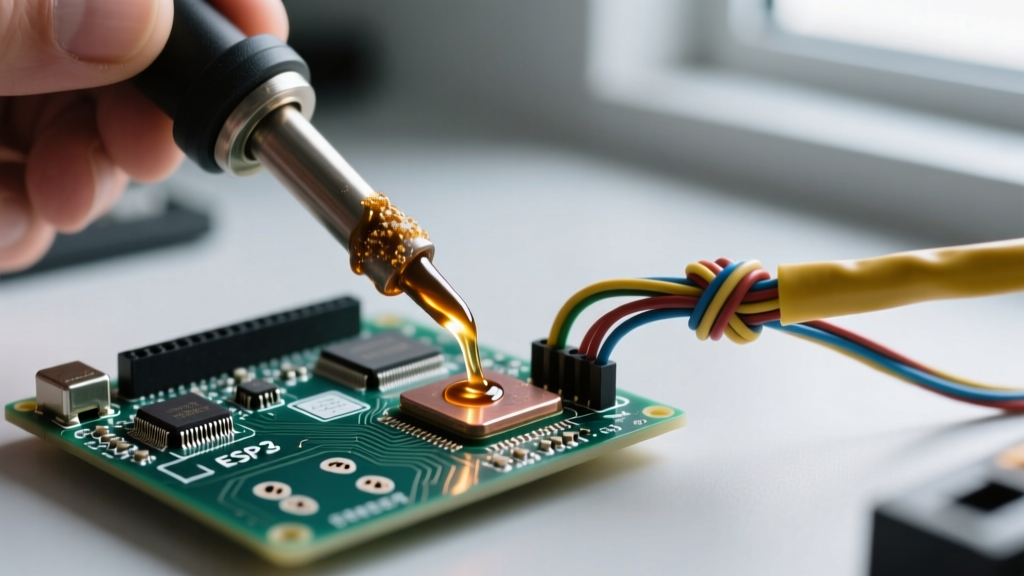
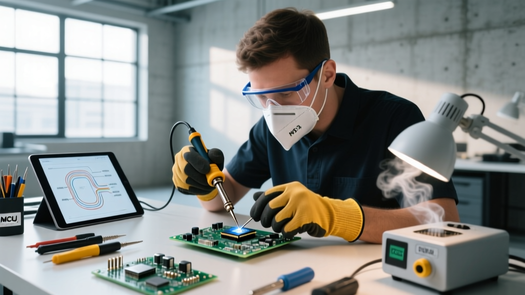
When soldering on a motherboard, you are not simply joining two pieces of metal; you are battling complex thermal dynamics. Modern PC and laptop motherboards feature 6 to 14 internal copper layers. These layers act as massive heat sinks, rapidly drawing thermal energy away from your soldering tip or hot air nozzle. If you approach motherboard repair with the same techniques used for simple single-layer hobby PCBs, you will inevitably face cold joints, lifted pads, or destroyed components.
In this comprehensive method comparison, we break down the three primary techniques for soldering on a motherboard: precision micro-soldering irons, hot air rework stations, and the professional hybrid preheating method. Whether you are replacing a blown 0402 SMD capacitor or reballing a complex BGA chipset, understanding the thermal limitations and strengths of each method is critical for success in 2026.
Method 1: Precision Soldering Irons (The Traditional Approach)
The soldering iron remains the foundational tool for any electronics workbench. However, when soldering on a motherboard, standard 40W to 60W ceramic heating elements often stall. When the tip touches a via connected to an internal ground plane, the temperature plummets, leading to prolonged dwell times that melt component housings and delaminate the FR-4 fiberglass substrate.
The Solution: Active Tip Technology
To overcome the thermal mass of multi-layer motherboards, professionals rely on active cartridge systems. The JBC CD-2BQE (retailing around $750) paired with C245 series cartridges is the current industry benchmark. In these systems, the heating element is integrated directly inside the copper tip, reducing the thermal transfer distance to mere millimeters.
- Recovery Time: Drops from 15 seconds (traditional) to under 2 seconds.
- Optimal Use Cases: Through-hole electrolytic capacitors, SOIC-8 BIOS chips, 0402/0603 SMD passives, and applying fresh solder to QFP pins.
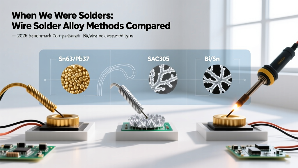
- Recommended Settings: 350°C for leaded Sn63/Pb37 solder; 380°C for lead-free SAC305 alloys.
Pro Tip: Never use a standard chisel tip for dense SMD work. Use a JBC C245-1129 (bent conical) or C245-903 (micro-blade) to access tight pitches without bridging adjacent pads.
Method 2: Hot Air Rework Stations (The SMD Standard)
You cannot physically solder a 64-pin QFN (Quad Flat No-leads) or a BGA (Ball Grid Array) chip with a standard iron. For components with hidden thermal pads or underneath-ball connections, hot air is mandatory. Hot air rework stations use convective heat transfer, melting all joints simultaneously to allow for safe component lifting.
Tooling and Airflow Dynamics
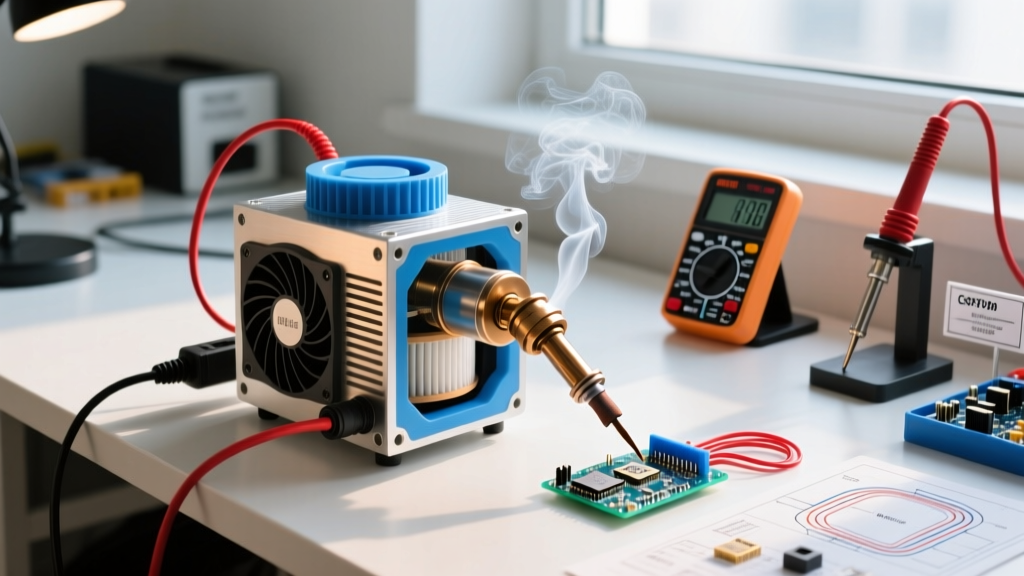
The Quick 861DW (approximately $350) is a staple for motherboard technicians due to its 1200W power output and brushless fan, which provides highly stable airflow without the pulsing vibration found in cheaper diaphragm pumps.
- Flux Application: Apply a generous amount of tacky flux, such as Amtech NC-559-V2-TF, to all pins. Flux is non-negotiable; it prevents oxidation and promotes even wetting.
- Nozzle Selection: Use a nozzle that closely matches the IC body size (e.g., a 12mm x 12mm nozzle for a 10mm QFN chip) to concentrate thermal energy and protect surrounding plastics.
- Temperature and Airflow: Set temperature to 360°C - 380°C. Keep airflow low (around 30-40%) to prevent blowing tiny 0201 resistors off the board.
Head-to-Head Comparison Matrix
Choosing the right method depends entirely on the component package and the board's copper density. Refer to the matrix below to guide your workflow.
| Feature | Precision Iron (JBC C245) | Hot Air (Quick 861DW) | Hybrid (Preheat + Air/Iron) |
|---|---|---|---|
| Best Component Types | SOIC, DIP, large SMD, through-hole | QFN, BGA, QFP, multi-pin ICs | Massive ground planes, BGA, server boards |
| Heat Transfer Method | Conduction (Direct contact) | Convection (Heated air) | Radiation (IR) + Convection/Conduction |
| Risk of Pad Lifting | Moderate (if dwell time is too long) | High (if prying before full reflow) | Low (board is uniformly saturated) |
| Skill Curve | Moderate | Steep | Expert |
| Avg. Equipment Cost | $500 - $800 | $250 - $500 | $1,000 - $1,800 |
Method 3: Hybrid Preheating (The Professional Standard)
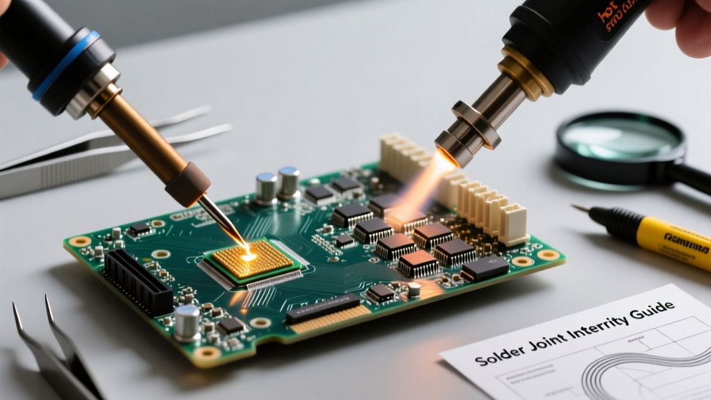
When soldering on a motherboard with heavy copper pours (such as GPU VRM phases or ATX 24-pin power connectors), neither an iron nor hot air alone is sufficient. Applying extreme localized heat to a cold board creates a severe thermal gradient. This gradient causes the FR-4 substrate to expand unevenly, leading to micro-fractures in internal vias and pad cratering.
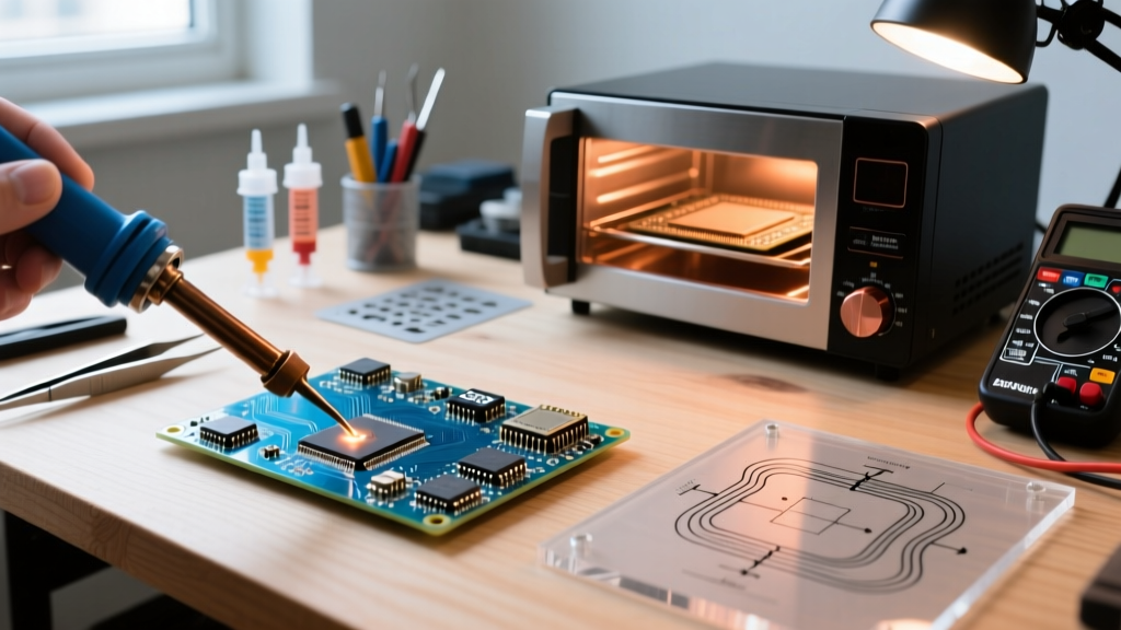
The professional standard involves using an IR (Infrared) preheater, like the Hakko FR-820, to raise the entire motherboard's ambient temperature to 100°C - 120°C before applying localized hot air or an iron. According to guidelines emphasized by the NASA Electronic Parts and Packaging (NEPP) Program, uniform preheating drastically reduces thermal shock to sensitive multi-layer ceramic capacitors (MLCCs) and ensures consistent solder reflow across high-mass joints.
Step-by-Step Preheating Workflow
- Step 1: Secure the motherboard flat on the preheater bed using high-temperature Kapton tape to prevent warping.
- Step 2: Ramp the preheater to 110°C over 3 minutes. Avoid rapid thermal ramping.
- Step 3: Once the board reaches thermal equilibrium, apply localized hot air at a reduced temperature (e.g., 300°C instead of 380°C) to remove the target IC.
- Step 4: Allow the board to cool naturally on the preheater bed. Never use compressed air or liquid coolants to force-cool a multi-layer PCB.
Critical Failure Modes When Soldering on a Motherboard
Even with the right tools, poor technique will destroy a motherboard. Be hyper-aware of these common failure modes:
1. Pad Cratering and Delamination
This occurs when a technician attempts to lift an SMD component with tweezers before the solder has fully transitioned to a liquid state. The mechanical force rips the copper pad away from the underlying fiberglass. Fix: Always gently nudge the component with tweezers; if it does not move freely with near-zero resistance, apply more heat and flux.
2. MLCC Thermal Cracking
Multi-Layer Ceramic Capacitors are highly susceptible to thermal shock. Touching a 400°C iron directly to a cold MLCC can cause microscopic internal cracks that fail weeks later under voltage load. The IPC standards for electronic assemblies strictly mandate controlled heating profiles to prevent dielectric fracturing in ceramic components.
3. Tombstoning
Common during hot air reflow of 0402 and 0201 resistors, tombstoning happens when one pad reaches reflow temperature before the other. The surface tension of the molten solder pulls the component upright. Fix: Use a wider hot air nozzle to ensure both pads heat simultaneously, and rely on high-quality solder paste like Chip Quik SMD4300AX10 which features a highly active flux core to promote even wetting.
Expert Verdict: Which Method Should You Choose?
There is no single 'best' method for soldering on a motherboard; the correct approach is dictated by the component geometry and the board's copper density. For general troubleshooting, replacing BIOS chips, and swapping blown capacitors, a high-end precision iron like the JBC CD-2BQE is unmatched in speed and safety. However, the moment you encounter a QFN power delivery IC or a BGA chipset, you must transition to hot air. For heavy-duty server motherboards or GPU core repairs, investing in an IR preheating station is not optional—it is a mandatory safeguard against catastrophic substrate damage.
Frequently Asked Questions
Can I use lead-free solder for motherboard repairs?
While OEMs use lead-free SAC305 solder to comply with RoHS directives, most independent repair technicians use leaded Sn63/Pb37 solder for rework. Leaded solder melts at a lower temperature (183°C vs 217°C), reducing thermal stress on the motherboard. According to metallurgical data from Kester Technical Resources, Sn63/Pb37 also provides a distinct eutectic transition, meaning it goes from solid to liquid instantly, reducing the risk of disturbed joints during cooling.
How do I clean flux residue after soldering on a motherboard?
Even 'no-clean' fluxes can leave conductive or corrosive residues if overheated. Clean the repaired area using 99% isopropyl alcohol (IPA) and a soft ESD-safe brush. For heavy tacky fluxes, a dedicated PCB cleaner like MG Chemicals Super Wash is highly effective.
What is the best solder wick for motherboard pad preparation?
Before installing a new IC, the pads must be perfectly flat. Use a high-purity copper wick, such as the Goot Wick CP-2015 (1.5mm width). The 1.5mm width is narrow enough to prevent accidental bridging on fine-pitch QFP chips while providing enough capillary action to absorb residual solder from the motherboard pads.