
The Dawn of Metallurgical Joining: Ancient Origins
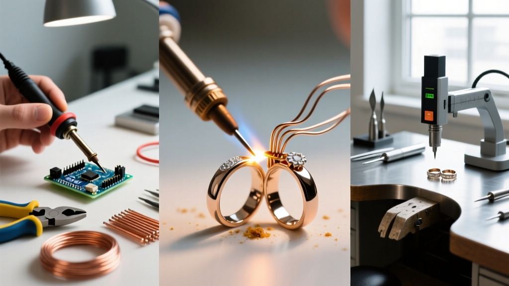
Long before the invention of the printed circuit board (PCB) or the semiconductor, early civilizations were already mastering the fundamentals of metallurgical joining. The history of soldering applications dates back over 5,000 years to ancient Mesopotamia and Egypt. Artisans in these regions utilized early forms of solder—primarily tin-lead and gold-silver-copper mixtures—to craft intricate jewelry, seal copper plumbing, and construct weapons.
Historical Insight: Archaeological evidence from the Tomb of Tutankhamun (circa 1323 BC) reveals the use of hard soldering (brazing) techniques to join gold alloys, requiring flux mixtures derived from animal fats and plant resins to prevent oxidation.
These ancient soldering applications were strictly mechanical and decorative. The metallurgical understanding was entirely empirical; smiths knew that adding tin to copper lowered the melting point, but the underlying crystalline phase changes remained a mystery until the advent of modern materials science.
The Industrial Era: Plumbing and the Tin-Lead Standard
As the Industrial Revolution mechanized manufacturing, the demand for reliable fluid and gas transport skyrocketed. In the 19th century, soldering applications expanded massively into plumbing and roofing. Plumbers utilized "wiped joints," a technique requiring a 50/50 tin-lead (Sn50Pb50) alloy. This specific composition was chosen because it possesses a wide plastic range (the temperature gap between the solidus and liquidus states), allowing the plumber to physically mold and wipe the molten solder over the joint before it fully solidified.
While highly effective for lead pipes, the toxicity of lead was poorly understood at the time. It wasn't until the late 20th century that the severe health implications of lead in potable water systems forced a complete paradigm shift in plumbing soldering applications, mandating lead-free alternatives like 95/5 tin-copper.
The Electronics Boom: Eutectic Alloys and Point-to-Point Wiring
The true turning point for modern electronics occurred in the 1920s and 1930s with the mass production of vacuum tube radios. Point-to-point wiring required a solder alloy that would melt and freeze rapidly to prevent heat damage to delicate components and to speed up assembly line production.
Materials scientists standardized the 63/37 tin-lead (Sn63Pb37) eutectic alloy. Unlike the 50/50 plumbing solder, the eutectic 63/37 mixture has a single melting point of exactly 183°C (361°F). It transitions instantly from liquid to solid without a plastic phase. This eliminated the risk of "disturbed joints"—a catastrophic failure mode where a component moves while the solder is in its semi-solid state, resulting in a grainy, high-resistance, and mechanically weak connection.
The PCB Revolution and Wave Soldering
By the 1950s, the invention of the printed circuit board transformed soldering applications from manual point-to-point wiring to automated batch processing. The introduction of wave soldering allowed entire PCBs to be passed over a standing wave of molten Sn63Pb37 solder, simultaneously forming hundreds of through-hole joints in seconds. This era also saw the establishment of early military standards (MIL-STD-2000), which eventually evolved into the modern IPC standards governing electronic assembly quality.
The RoHS Turning Point: Lead-Free Soldering Applications
The most disruptive event in the history of soldering applications occurred on July 1, 2006, when the European Union enforced the Restriction of Hazardous Substances (RoHS) Directive. This legislation effectively banned lead in commercial electronics, forcing the global industry to adopt lead-free alloys almost overnight.
The transition was far from seamless. The industry largely settled on SAC305 (96.5% Tin, 3.0% Silver, 0.5% Copper). However, SAC305 introduced new challenges:
- Higher Thermal Profiles: SAC305 melts at 217°C–220°C, requiring peak reflow temperatures of 245°C–260°C, which stressed early surface-mount components and caused PCB delamination.
- Wetting Issues: Lead-free solder exhibits poorer wetting characteristics, leading to increased occurrences of "tombstoning" (where surface-mount components stand on one end due to uneven surface tension).
- Tin Whiskers: The absence of lead in pure tin finishes increased the susceptibility to tin whiskers—microscopic crystalline structures that grow from the solder joint and cause catastrophic short circuits in high-reliability aerospace and medical devices.
Alloy Comparison Matrix: Historical vs. Modern
| Alloy Designation | Composition | Melting Point | Primary Application Era | Key Characteristics |
|---|---|---|---|---|
| Sn50Pb50 | 50% Sn, 50% Pb | 183°C - 215°C | 19th Century Plumbing | Wide plastic range, ideal for wiped joints. |
| Sn63Pb37 | 63% Sn, 37% Pb | 183°C (Eutectic) | 1950s - 2006 Electronics | Instant freeze, excellent wetting, shiny finish. |
| SAC305 | 96.5% Sn, 3% Ag, 0.5% Cu | 217°C - 220°C | 2006 - Present (Standard) | RoHS compliant, higher thermal stress, prone to drop-shock failure. |
| SN100C | 99.3% Sn, 0.7% Cu, Ni, Ge | 227°C | 2015 - Present (Wave) | Cost-effective, dross-reduction, excellent for wave soldering. |
Modern Soldering Applications in 2026: Micro-Joining and Laser
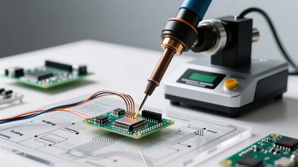
As we navigate the electronics landscape of 2026, the miniaturization of components has pushed traditional soldering applications to their physical limits. The industry is now routinely assembling 01005 (0.4mm x 0.2mm) and even 008004 (0.25mm x 0.125mm) metric chip components. At this scale, a standard 0.5mm soldering iron tip is essentially a blunt instrument.
To address these micro-joining requirements, modern assembly relies heavily on advanced reflow techniques and laser soldering. Laser soldering applies highly localized thermal energy (typically using 910nm or 1064nm diode lasers) to a specific joint in milliseconds. This prevents thermal damage to adjacent heat-sensitive substrates, such as flexible printed circuits (FPCs) used in modern wearables and medical implants.
Furthermore, the Surface Mount Technology Association (SMTA) has documented a massive shift toward Type 5 and Type 6 solder pastes (with powder mesh sizes ranging from 15 microns down to 5 microns) to accommodate the ultra-fine stencil apertures required for 2026's high-density interconnect (HDI) boards.
Buyer’s Guide: Selecting Alloys for Specific Applications Today
Understanding the historical evolution of soldering applications is crucial for selecting the right materials for your current projects. Here is a practical breakdown of what to buy based on your specific needs in the modern market:
1. For Hobbyist and Prototyping PCB Assembly
If you are not bound by commercial RoHS compliance, leaded Sn63Pb37 remains the undisputed king of hand soldering. It requires lower iron temperatures (320°C - 350°C tip temp), flows beautifully, and yields shiny, easily inspectable joints.
- Top Pick: Kester 245 (63/37) No-Clean Wire Solder.
- Estimated Cost (2026): $35 - $45 per 1lb spool.
- Best For: Through-hole components, point-to-point wiring, and DIY repairs.
2. For Commercial and RoHS-Compliant Production
For commercial products destined for global markets, you must use lead-free alloys. While SAC305 is standard for reflow, it can be harsh on hand-soldering iron tips due to the high silver content causing rapid tip corrosion.
- Top Pick: Senko SN100C (Lead-Free, Tin-Copper-Nickel-Germanium).
- Estimated Cost (2026): $60 - $75 per 1lb spool.
- Best For: Commercial hand-soldering, wave soldering pots. The addition of Nickel and Germanium drastically reduces dross formation and improves wetting compared to standard SAC alloys.
3. For High-Temperature and Harsh Environment Applications
Automotive and aerospace applications often require joints that can withstand continuous operating temperatures exceeding 150°C. Standard SAC305 will suffer from creep and fatigue under these conditions.
- Top Pick: Indalloy 151 (92.5% Sn, 7.5% Pb - note: requires RoHS exemption) or high-silver SAC405 for lead-free mandates.
- Estimated Cost (2026): $80 - $120+ per spool (Highly volatile based on silver spot prices).
- Best For: Under-hood automotive electronics, power supply modules, and high-vibration environments.
Conclusion
The evolution of soldering applications is a testament to human engineering—scaling from the brute-force metallurgical joins of ancient Egyptian tombs to the microscopic, laser-reflowed joints of 2026's quantum computing hardware. By understanding the metallurgical history and the specific failure modes of different alloys, makers, engineers, and procurement specialists can make highly informed decisions, ensuring their electronic assemblies survive both the test of time and the rigors of modern operation.