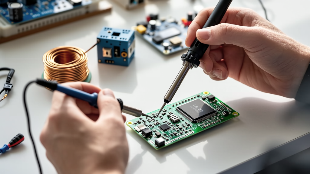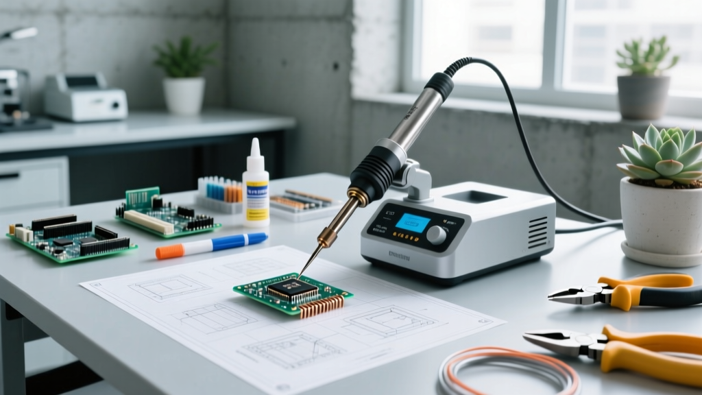

The Physics of Fluxless Joining: Acoustic Cavitation
For decades, electrical engineers and metallurgists have battled the tenacious oxide layers that form on metals like aluminum, as well as the inherently non-wettable surfaces of glass and advanced ceramics. Traditional chemical fluxes (RMA, RA, or no-clean) are entirely ineffective on aluminum oxide (Al2O3) or silicon dioxide, forcing manufacturers to rely on expensive plasma pre-treatment, aggressive acid washes, or specialized vacuum furnaces. Enter ultrasonic soldering—a solid-state acoustic process that eliminates the need for chemical fluxes by using high-frequency mechanical vibrations to shatter oxide layers at the microscopic level.
At the core of an ultrasonic soldering iron is a piezoelectric transducer stack that converts electrical energy into mechanical vibrations, typically oscillating between 20 kHz and 60 kHz. When the heated soldering tip (usually machined from a titanium alloy) contacts the molten solder pool on the substrate, it introduces acoustic waves into the liquid metal. This triggers acoustic cavitation: the rapid formation and violent collapse of microscopic vacuum bubbles within the molten solder. The implosion of these bubbles generates localized micro-jets of liquid metal traveling at hundreds of meters per second, effectively blasting away the oxide layer and allowing the active elements in the solder (like Titanium or Indium) to bond directly with the bare substrate.
Expert Insight: According to research documented by The Welding Institute (TWI), the localized temperatures during cavitation bubble collapse can momentarily exceed 5,000°C, though the bulk solder temperature remains strictly at the alloy's liquidus point, preventing thermal damage to sensitive components.
The 4-Pillar Decision Matrix: Is Ultrasonic Right for You?
Investing in ultrasonic soldering equipment is a significant capital expenditure. To determine if this technology belongs on your production floor or in your R&D lab, evaluate your process against the following matrix.
| Evaluation Pillar | Traditional Flux Soldering | Ultrasonic Soldering | Verdict |
|---|---|---|---|
| Substrate Material | Copper, Brass, Nickel, Gold, Silver | Aluminum, Glass, Quartz, Alumina, LTCC, Diamond | Choose Ultrasonic for non-wettable or heavy-oxide materials. |
| Environmental & Cleaning | Requires aqueous washing, saponifiers, DI water, and wastewater disposal. | 100% Fluxless. Zero VOCs, zero post-solder cleaning required. | Choose Ultrasonic if cleanroom standards or environmental compliance (RoHS/REACH) are strict. |
| Production Volume | Highly scalable via wave, reflow, or selective soldering. | Best for low-to-medium volume, specialized prototyping, or manual rework. | Choose Traditional for high-volume consumer PCBs; Ultrasonic for specialized sensors/aerospace. |
| Thermal Budget | Standard profiles; flux aids heat transfer. | Requires precise thermal management; acoustic energy adds localized heat. | Choose Ultrasonic for thick thermal mass substrates (e.g., IGBT baseplates). |
Material-Specific Edge Cases & Alloy Selection
Ultrasonic soldering is not a one-size-fits-all solution. The success of the joint relies heavily on pairing the correct acoustic frequency with a specifically formulated active solder alloy. Standard SAC305 (Sn96.5/Ag3.0/Cu0.5) will not work, as it lacks the active elements required to chemically bond to the freshly exposed substrate once the oxide is blasted away.
Aluminum and Heavy Oxide Metals
When joining aluminum busbars or heat sinks, the oxide layer (Al2O3) reforms in milliseconds upon exposure to air. Therefore, the cavitation must occur underneath the molten solder pool to prevent immediate re-oxidation. For this, a lower frequency of 20 kHz with a high amplitude (up to 50 microns peak-to-peak) is required. The recommended alloy is a Tin-Silver-Copper-Titanium matrix, such as S-Bond Technologies' 220M series, which contains roughly 1-2% Titanium. The titanium reacts with the bare aluminum to form intermetallic compounds (IMCs), creating a bond with shear strengths often exceeding 40 MPa.
Glass, Quartz, and Advanced Ceramics
Soldering to glass or Low-Temperature Co-fired Ceramics (LTCC) presents a different challenge: brittleness. The violent micro-jets generated at 20 kHz will cause micro-fractures, chipping, or catastrophic shattering of the substrate. For these applications, you must step up to a 60 kHz ultrasonic generator, which provides a much finer, lower-amplitude vibration (approx. 10-15 microns). Furthermore, Titanium-based active solders require temperatures above 250°C, which may exceed the glass transition limits of certain optical assemblies. Instead, engineers utilize Indium-based active alloys (e.g., Indium 5.7 or Sn-In-Ti formulations) which melt between 120°C and 170°C, preserving the structural integrity of fragile optical and RF components.
CapEx vs. OpEx: The True Cost of Ownership
When building a business case for ultrasonic soldering, lab managers must look beyond the initial hardware cost and evaluate the total cost of ownership (TCO) over a 5-year horizon.
- Capital Expenditure (CapEx): A high-quality handheld ultrasonic soldering system (generator, transducer, and titanium tip) from manufacturers like Teca-Print or Sonics & Materials typically ranges from $4,500 to $8,500. Fully automated, CNC-integrated ultrasonic soldering workstations designed for semiconductor die-attach or large aerospace panels can range from $35,000 to over $75,000.
- Consumables (OpEx): Active solder wires and pastes are significantly more expensive than standard electronics solder. A 1 lb spool of Sn-Ag-Cu-Ti active solder wire can cost between $120 and $250, compared to $35 for standard SAC305. However, you completely eliminate the cost of chemical fluxes, saponifiers, and cleaning solvents.
- Hidden Costs (Maintenance): The very mechanism that makes ultrasonic soldering effective—cavitation—also erodes the titanium tip. Expect to replace titanium tips every 40 to 80 hours of active arc-on time. Replacement tips cost between $150 and $350 each, depending on the geometry and manufacturer.
Critical Failure Modes to Anticipate
Operators transitioning from standard thermal irons to ultrasonic systems frequently encounter specific failure modes due to a misunderstanding of acoustic mechanics. Be aware of the following edge cases:
- Acoustic Decoupling (Operator Error): Unlike standard soldering where applying downward pressure improves thermal transfer, pressing down hard on an ultrasonic tip dampens the vibration. This shifts the resonant frequency of the piezoelectric stack, causing the generator's phase-locked loop (PLL) to lose tracking. This results in an impedance fault alarm or, in severe cases, the physical cracking of the PZT crystals inside the handpiece.
- Substrate Delamination: When soldering to multi-layer ceramic capacitors (MLCCs) or HTCC/LTCC modules, excessive acoustic energy can propagate through the substrate and delaminate internal buried traces. Always perform a cross-section analysis and dye-penetrant test on prototype joints before committing to a production frequency profile.
- Active Element Depletion: If the solder pot or wire is held at liquidus temperatures for extended periods without being agitated, the heavier active elements (like Titanium) can segregate or oxidize at the surface of the bath, leading to 'dead' solder that fails to wet the substrate despite ultrasonic agitation.
Final Verdict: Should You Make the Switch?
Ultrasonic soldering is not a replacement for selective wave soldering on standard FR-4 PCB assemblies; the CapEx and tip wear make it economically unviable for high-volume consumer electronics. However, if your manufacturing or R&D roadmap involves power electronics (SiC/GaN die-attach), automotive aluminum busbars, aerospace RF ceramic packages, or hermetic glass-to-metal seals, the decision framework heavily favors ultrasonic investment.
By eliminating the variability of chemical flux activation, removing the need for multi-stage aqueous cleaning lines, and enabling direct metallurgical bonds to previously 'unsolderable' materials, ultrasonic soldering transitions from a niche laboratory curiosity to an indispensable pillar of advanced electronic manufacturing. For teams working with next-generation wide-bandgap semiconductors and advanced composite substrates, the ROI is typically realized within 14 to 18 months through reduced scrap rates and eliminated chemical compliance overhead.