
The Industrial Shift: Why Hobbyist Methods Fail in Production
When transitioning from hobbyist prototyping to high-reliability manufacturing, following a strict soldering step by step protocol is not merely a recommendation—it is an IPC-mandated requirement for Class 3 assemblies. In aerospace, medical devices, and automotive electronics, a single cold joint or insufficient intermetallic compound (IMC) layer can result in catastrophic field failures costing millions in recalls. Hobbyists often rely on visual cues and basic 60W ceramic heaters, but industrial technicians must manage thermal mass, moisture sensitivity levels (MSL), and precise metallurgical wetting angles.
This guide details the professional, high-reliability approach to manual PCB assembly. We will break down the exact metallurgy, thermal profiling, and inspection criteria required to meet the stringent demands of modern electronics manufacturing in 2026.
IPC-A-610 Class 3 Definition: 'High-Performance Electronic Products' includes products where continued high performance or extended life is critical, and downtime cannot be tolerated. The end-use environment may be uncommonly harsh, and the equipment must function when required, such as life support or flight control systems.
Pre-Assembly: Environmental and Material Controls
Before an iron ever touches a pad, industrial facilities enforce strict environmental controls. Moisture trapped inside plastic-encapsulated ICs can vaporize during reflow or manual spot-heating, causing the 'popcorn effect' (delamination and micro-cracking).
Moisture Sensitivity and Baking
Components rated MSL 3 or higher must be stored in dry cabinets (maintained at <5% relative humidity) or baked prior to assembly. According to SMTA guidelines, baking typically occurs at 125°C for 8 to 24 hours, depending on package thickness. Soldering a moisture-compromised BGA or QFN component by hand will almost certainly fracture the internal die attach.
ESD and Surface Preparation
All manual assembly stations must be grounded via a 1-megohm current-limiting resistor to an ESD common point ground. Technicians use ionizing blowers to neutralize static charges on FR-4 laminates and polyimide flex circuits before applying flux. The PCB surface must be free of oxidation; if the board has been exposed to ambient air for more than 72 hours, a mild organic acid (OA) preclean or plasma desmear is required to ensure proper wetting.
Soldering Step by Step: The High-Reliability Protocol
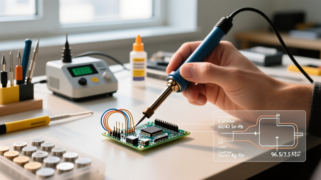
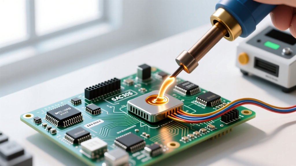
The following sequence represents the industry-standard manual soldering process for through-hole and surface-mount components, optimized for lead-free SAC305 (Sn96.5/Ag3.0/Cu0.5) alloys, which dominate the 2026 manufacturing landscape.
- Step 1: Thermal Preparation and Tip Tinning
Select a tip geometry that maximizes contact area with both the component lead and the PCB pad. For a standard 0805 surface-mount pad, a micro-chisel or bevel tip (e.g., JBC C115-112 or Weller RT3) is ideal. Before approaching the board, apply a small amount of fresh solder to the tip. This 'tinning' layer acts as a thermal bridge, drastically reducing the thermal resistance between the iron and the joint. Set the station to 350°C - 360°C for SAC305 wire. - Step 2: Targeted Flux Application
Even if using flux-cored wire, applying an external no-clean or rosin mildly activated (RMA) flux gel (such as Kester HF-995 or Indium SMF-230) ensures the oxides are fully dissolved. Apply a volume roughly 20% larger than the joint area. The flux must activate (turn clear and bubble slightly) before the solder is introduced. - Step 3: Simultaneous Heating (The 45-Degree Rule)
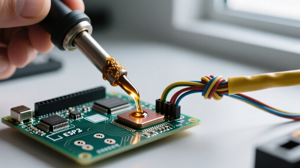
Place the tinned tip at a 45-degree angle so it simultaneously contacts the component lead and the copper pad. Hold for 1 to 2 seconds. The goal is to bring both metallic surfaces above the liquidus temperature of the solder (217°C for SAC305) before introducing the wire. Never use the iron to melt the solder and then 'carry' it to the joint; this depletes the flux and creates a cold, oxidized joint. - Step 4: Feed and Reflow
Feed the solder wire (typically 0.031' diameter for standard joints, 0.015' for micro-BGA repair) directly into the intersection of the pad and lead, not onto the iron tip. The heat conducted through the metal surfaces will melt the wire instantly. Feed until a smooth, concave fillet forms. For through-hole components, aim for 100% barrel fill and a top-side meniscus that wets the entire annular ring. - Step 5: Controlled Cooling and Inspection
Remove the solder wire first, then the iron. The joint must remain perfectly still during the solidification phase (typically 2-4 seconds). Disturbing a joint while the alloy is transitioning from a paste to a solid state causes a 'disturbed joint'—characterized by a grainy, dull appearance and microscopic fractures in the IMC layer.
The Metallurgy of the Joint: Understanding the IMC Layer
Professional technicians understand that soldering is not merely 'gluing' metal with metal; it is a metallurgical welding process. When molten tin comes into contact with a copper pad, it dissolves a microscopic layer of the copper and forms an Intermetallic Compound (IMC), primarily Cu6Sn5 (eta phase) and Cu3Sn (epsilon phase).
According to metallurgical studies published by Indium Corporation, the ideal IMC thickness for a reliable joint is between 1 and 3 microns. If the iron temperature is too low or the dwell time too short, the IMC layer is too thin, resulting in poor tensile strength. Conversely, excessive heat or prolonged rework bakes the joint, causing the IMC layer to grow beyond 5 microns. A thick IMC layer is highly brittle and will easily fracture under thermal cycling or mechanical shock—a critical failure mode in automotive and aerospace applications.
Equipment Matrix: Industrial vs. Prosumer Stations
Achieving the precise thermal control required for the soldering step by step protocol above demands active tip-sensing technology. Traditional ceramic heating elements suffer from thermal lag, dropping up to 40°C when touching a heavy ground plane. Modern industrial stations use direct-heater cartridges where the tip and heater are a single integrated unit, ensuring near-instant thermal recovery.
| Station Model | Heater Technology | Max Power | Thermal Recovery | Approx. Cost (2026) |
|---|---|---|---|---|
| JBC CD-2BQE | Integrated Cartridge | 130W | < 2 Seconds | $850 |
| Weller WXD2 | Active Tip (RT Series) | 200W (Total) | < 3 Seconds | $720 |
| Hakko FX-952 | Composite Ceramic | 70W | 5-8 Seconds | $380 |
| Metcal MX-5200 | SmartHeat (Induction) | 80W | Instant (Curie Point) | $950 |
While the Hakko FX-952 remains a staple in high-end prosumer and light commercial repair shops, facilities building Class 3 medical or aerospace hardware overwhelmingly standardize on JBC or Metcal systems. Metcal's SmartHeat technology is particularly notable for high-reliability work: it uses RF induction and relies on the Curie point of the tip's ferromagnetic alloy to self-regulate temperature, eliminating the need for manual calibration and preventing accidental overheating of sensitive components.
Common Industrial Failure Modes and Root Causes
Even when following a strict protocol, process deviations occur. IPC standards categorize defects into process indicators and true defects. Below are the most common failure modes encountered in manual assembly and their root causes:
- Cold Joints (Dull, Grainy Appearance): Caused by insufficient heat transfer. The solder solidified before fully wetting the copper surfaces. Prevention: Increase tip contact area, verify station calibration, and ensure simultaneous heating of pad and lead.
- Solder Balls and Bridging: Often caused by excessive flux boil-off or using a solder wire diameter that is too thick for the pitch of the component. Prevention: Switch to a low-splatter no-clean flux formulation and reduce wire diameter to 0.015' for fine-pitch QFPs.
- Pad Lift / Delamination: The copper pad separates from the FR-4 substrate. Caused by excessive dwell time (usually >5 seconds) or using a tip temperature exceeding 400°C. Prevention: Limit manual contact time to 3 seconds maximum per joint. Use pre-heaters for multi-layer boards with heavy internal ground planes.
- Icicles and Protrusions: Excess solder that forms a spike, risking short circuits. Caused by poor wetting due to oxidized pads or insufficient flux activation. Prevention: Apply additional liquid flux and use a clean, tinned wick to desolder and re-flow the joint.
Conclusion
Mastering the industrial approach to manual assembly requires abandoning the 'melt and stick' mentality. By treating the soldering step by step process as a controlled metallurgical event—governed by strict environmental prep, precise thermal profiling, and rigorous IPC-A-610 inspection criteria—technicians can produce joints that withstand the harshest operational environments. Investing in active-sensing equipment and understanding the underlying chemistry of the IMC layer separates the professional assembly house from the amateur workbench.