
From Vacuum Tubes to 01005 Components: The Micro-Soldering Revolution
Micro-soldering is the meticulous art and science of joining electronic components measured in fractions of a millimeter. Today, technicians routinely repair smartphone logic boards featuring 0.4mm pitch Ball Grid Arrays (BGAs) and 01005 passive components (0.4mm x 0.2mm). However, the journey to this level of precision was neither fast nor straightforward. Understanding the history and evolution of micro-soldering is not just an academic exercise; it directly informs the tools, techniques, and capital investments modern electronics technicians and engineers must make in 2026.
By tracing the lineage of miniaturization, buyers can better understand why certain technologies—like direct-heat cartridge soldering irons and high-magnification trinocular microscopes—have completely replaced the bulky, slow-heating ceramic stations of the late 20th century.
The Genesis of Miniaturization (1940s–1970s)
The demand for smaller electronics was initially driven by military and aerospace applications, followed closely by the commercial hearing aid market in the 1950s. Early "miniature" work involved sub-miniature vacuum tubes and the first generation of discrete transistors. Soldering at this scale relied on finely ground copper tips attached to massive, transformer-based irons. Temperature control was virtually non-existent; operators relied on visual cues and the melting speed of rosin-core solder to gauge heat.
The true paradigm shift occurred with the invention of the integrated circuit (IC) and the subsequent birth of Surface Mount Technology (SMT). By the late 1970s, the electronics industry began transitioning from Through-Hole Technology (THT) to surface-mounted components to save space and reduce manufacturing costs. This transition forced the soldering industry to invent the first dedicated micro-soldering tools, including early hot-air pencils and fine-wire thermocouple-equipped irons.
The SMT Boom and the Birth of Modern Rework (1980s–2000s)
As consumer electronics exploded in the 1980s and 1990s, component sizes shrank from 1206 (3.2mm x 1.6mm) to 0805 and eventually 0603. The Surface Mount Technology Association (SMTA) and IPC standards committees began formalizing workmanship requirements, pushing tool manufacturers to develop more precise thermal recovery systems.
During this era, brands like Hakko and Weller dominated the market with ceramic heating elements. While revolutionary at the time, these early SMT stations suffered from a critical flaw: thermal lag. The sensor was located deep inside the ceramic core, far from the tip. When a technician touched a 0805 capacitor, the tip temperature would plummet, and the station would take several seconds to recover, often leading to cold solder joints or, conversely, thermal damage from overshooting the target temperature.
The Evolution Matrix: Component Sizes and Tooling
| Era | Standard Component Size | Typical Joint Pitch | Primary Soldering Technology | Visual Aid |
|---|---|---|---|---|
| 1970s | Discrete Transistors / Early DIP | 2.54mm (100 mil) | Transformer Irons / Ungar Resistive | Naked Eye / Magnifying Glass |
| 1990s | 1206 / 0805 / SOIC | 1.27mm to 0.8mm | Ceramic Heater Stations (Hakko 936) | Desktop Magnifying Lamp |
| 2010s | 0402 / QFN / Early BGA | 0.5mm to 0.4mm | Direct-Heat Cartridge (JBC T245) | Stereo Zoom Microscope (10x-20x) |
| 2026 | 01005 / 0.3mm Pitch BGA | 0.3mm to 0.15mm | Smart Active-Tip / Nano-Stations | 4K Digital / High-Res Trinocular |
The Modern Era: Direct Heating and the 01005 Challenge (2010s–Present)
The introduction of the smartphone completely rewrote the rules of micro-soldering. Logic boards became multi-layered, high-density interconnect (HDI) nightmares packed with 0201 and 01005 passives. The old ceramic heaters were rendered obsolete for high-end rework.
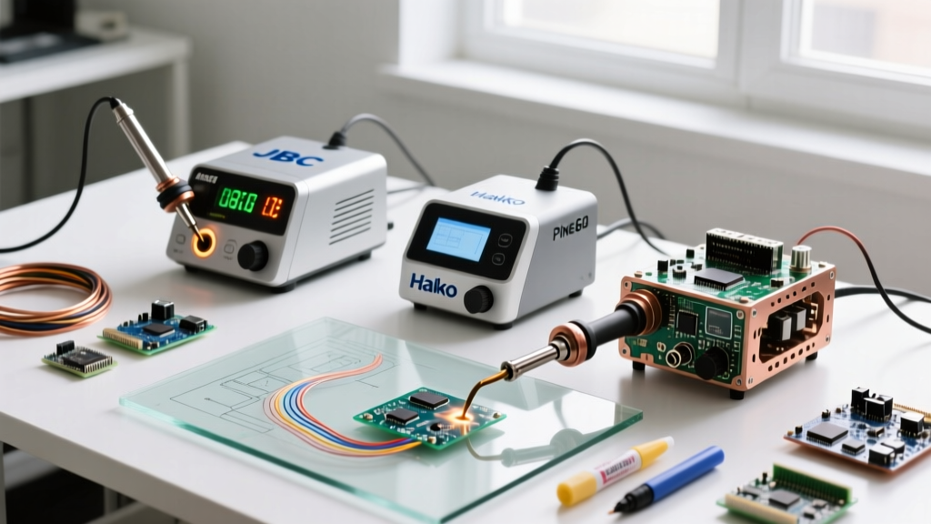
The industry standard shifted toward direct-heat cartridge systems, pioneered by companies like JBC Tools. In these systems, the heating element and the thermocouple are integrated directly into the tip itself. This allows for thermal recovery times measured in milliseconds rather than seconds. When a 0.1mm micro-tip touches a copper ground plane, the station instantly detects the heat sink effect and pumps maximum current to the tip, maintaining a stable 350°C without overshooting.
2026 Micro-Soldering Buyer’s Guide: Building Your Bench
If you are setting up a micro-soldering station today for board-level repair, aerospace prototyping, or advanced DIY, your buying decisions must reflect the demands of modern HDI boards. Here is the definitive breakdown of what to purchase.
1. The Soldering Station: Cartridge vs. Ceramic
- The Premium Standard: JBC CD-2BQF (approx. $750)
Paired with the T245 handle, this is the undisputed king of micro-soldering. You will need specialized tips like the C245-001 (0.1mm conical) for jumper wire installation and the C245-116 (0.6mm blade) for dragging 0.4mm pitch QFP chips. The instant heat recovery prevents pad lifting on fragile smartphone logic boards. - The Budget Alternative: Hakko FX-951 (approx. $350)
While older in design, the FX-951 with T15 series tips remains a workhorse for components 0402 and larger. However, for 0201 and 01005 work, the thermal mass of the T15 tips struggles to maintain wetting without excessive dwell time, increasing the risk of flux burnout.
2. Optics: Why Stereo Zoom is Non-Negotiable
You cannot micro-solder what you cannot see. The human eye resolves down to about 0.1mm under perfect conditions, but identifying a 0.05mm solder bridge on a BGA requires magnification.
Buyer Tip: Avoid cheap digital USB microscopes for active soldering. The latency (even at 60fps) causes hand-eye coordination drift, leading to slipped tips and severed traces. Always opt for optical stereo zoom.
- AmScope SM-4TP (approx. $280): A 7x-45x continuous zoom trinocular stereo microscope. The trinocular head allows you to mount a camera for recording or streaming without sacrificing your binocular viewing plane.
- Leica A60 F (approx. $2,800+): For professional labs requiring flawless edge-to-edge clarity and ergonomic strain reduction over 8-hour shifts. The apochromatic lens correction eliminates the color fringing seen on cheaper optics when viewing highly reflective solder joints.
3. Hot Air Rework: Precision Airflow
Micro-soldering relies heavily on hot air for BGA removal and flex-cable desoldering. The Quick 861DW (approx. $300) remains the benchmark. Its 1000W brushless fan provides stable airflow without the vibration that knocks microscopic components off their pads. For micro-BGA work, pair it with 12mm and 8mm round nozzles to concentrate heat strictly on the component body, shielding surrounding micro-plastics and connectors.
Critical Consumables for Sub-Millimeter Work
Your tools are only as good as your chemistry. In micro-soldering, flux is not optional; it is the primary driver of joint reliability.
- Flux: Use a high-tack, no-clean gel flux like Amtech NC-559-V2-TF or Kingbo RMA-223 (for budget repairs). High tack prevents 01005 components from blowing away under hot air.
- Solder Wire: Stock 0.3mm diameter wire is too thick for 0201 pads. Buy 0.15mm Kester or Mechanic leaded (63/37) solder wire. Leaded solder melts at 183°C, drastically reducing the thermal stress on multi-layer ceramic capacitors (MLCCs) compared to SAC305 lead-free alloys (217°C).
- Desoldering Wick: Standard 2.5mm wick will rip micro-pads off the board. Use Goot Wick CP-2015 (1.5mm width) impregnated with ultra-pure rosin to gently wick away residual solder from 0.3mm pitch BGA pads without scrubbing.
Real-World Failure Modes and Edge Cases
Even with the best 2026 equipment, micro-soldering presents unique failure modes that buyers and technicians must anticipate:
Tombstoning on 01005 Passives
The Issue: A capacitor stands on one end during reflow, resembling a tombstone.
The Cause: Uneven heating or asymmetrical pad design causes one side of the component to wet before the other. The surface tension of the molten solder pulls the component upright.
The Fix: When hand-soldering, pre-tin only one pad. Place the component with tweezers, heat the pre-tinned pad to secure it, and then solder the second pad. Never apply hot air directly to a single 01005 without a surrounding thermal mass to equalize heating.
BGA Pad Cratering
The Issue: The epoxy resin beneath the copper BGA pad fractures, causing an intermittent open circuit that is nearly impossible to detect with a standard multimeter.
The Cause: Mechanical stress (prying a chip off before all solder spheres are fully molten) or extreme thermal gradients.
The Fix: Never use a spudger to pop off a BGA. Use a vacuum pickup pen (like the JBC NE-2) to lift the chip only after the flux has fully liquefied and the chip exhibits the "dancing" effect of surface tension.
Flex Cable Delamination
The Issue: The polyimide layers of an FPC (Flexible Printed Circuit) separate, exposing internal copper traces to shorting.
The Cause: Applying hot air exceeding 320°C for more than 5 seconds directly to the flex substrate.
The Fix: Use Kapton tape to mask the flex cable, leaving only the solder joints exposed. Apply a heat sink (like a copper coin or aluminum clip) to the base of the flex to draw thermal energy away from the delicate substrate.
Conclusion: Investing in the Craft
The evolution of micro-soldering from the clumsy transformer irons of the 1960s to the millisecond-responsive smart stations of today mirrors the exponential shrinking of Moore’s Law. As components continue to shrink and board densities increase, the barrier to entry for board-level repair and micro-assembly relies entirely on precision tooling. By investing in direct-heat cartridge stations, high-quality optical magnification, and sub-millimeter chemistry, technicians equip themselves to handle the microscopic demands of modern electronics, ensuring reliability in an era where a single misplaced micron of solder can mean the difference between a functioning device and a dead board.