
The Core Dilemma: Internal SOPs vs. IPC Certification
As electronic assemblies shrink and operate in increasingly harsh environments, the margin for soldering errors approaches zero. For Electronics Manufacturing Services (EMS) providers and hardware startups scaling into production, a critical operational crossroads emerges: should you rely on internal Standard Operating Procedures (SOPs), or formally adopt IPC J-STD-001 soldering compliance? When evaluating J Std 001 soldering requirements, manufacturers must weigh the rigorous demands of the standard against the tangible ROI of reduced field failures and expanded market access.
The IPC J-STD-001 standard, officially titled 'Requirements for Soldered Electrical and Electronic Assemblies,' is the globally recognized benchmark for soldering processes, materials, and quality criteria. In 2026, with the proliferation of high-density interconnect (HDI) boards and 01005 micro-components, homegrown SOPs are rarely sufficient to guarantee reliability in mission-critical applications. However, full facility certification and operator training represent a significant capital expenditure. This decision framework will help you determine if, when, and how to implement J-STD-001 in your production pipeline.
Understanding the Three Product Classes
Before calculating costs, you must define your target reliability tier. J-STD-001 categorizes assemblies into three distinct classes, each with escalating inspection criteria:
- Class 1 (General Electronic Products): Focuses primarily on completed assembly functionality. Suitable for consumer toys, basic lighting, and non-critical disposable electronics. Cosmetic solder defects are permissible if they do not impair function.
- Class 2 (Dedicated Service Electronic Products): Requires continued performance and extended life, though uninterrupted service is not critical. Most commercial computing, telecommunications, and automotive infotainment systems fall here. Plated Through Hole (PTH) barrel fill requirements sit at 75%.
- Class 3 (High-Performance Electronic Products): Demands strict adherence to operational parameters with zero tolerance for downtime. Includes medical life-support, aerospace, and military applications. PTH barrel fill mandates 100% on terminals on both sides, and wetting angles must be meticulously controlled.
The 2026 J-STD-001 Decision Matrix
Use the following matrix to determine your baseline requirement for formal J-STD-001 adoption versus internal quality management.
| Operational Scenario | Primary Product Class | Recommended Framework | Justification & ROI |
|---|---|---|---|
| Prototyping & Hobbyist Scaling | Class 1 / Unclassified | Internal SOPs + IPC-A-610 Visual Reference | High cost of CIS training outweighs low-volume risk. Focus on basic wetting and thermal management. |
| Mid-Volume Consumer IoT | Class 2 | Hybrid: Internal SOPs aligned to J-STD-001 | Formal certification may be overkill, but aligning SOPs to Class 2 criteria reduces RMA rates by up to 18%. |
| Automotive & Industrial Controls | Class 2 / Class 3 | Full Facility J-STD-001 Certification | OEM contracts in these sectors mandate certified operators. Non-compliance results in immediate vendor disqualification. |
| MedTech & Aerospace | Class 3 | Strict J-STD-001 + AS9100/ISO 13485 Integration | Liability and life-safety regulations require traceable, certified processes. ROI is measured in risk mitigation, not just yield. |
Financial and Operational Impact (2026 Pricing)
Transitioning to a compliant J-STD-001 facility is not merely a paperwork exercise; it requires specialized tooling and certified personnel. Here is a realistic breakdown of the capital and operational expenditures required in 2026.
Personnel Certification Costs
To be officially compliant, your line operators and inspectors must hold active Certified IPC Specialist (CIS) credentials. According to EPTAC's training modules, a standard 4-day CIS course for J-STD-001 averages $1,950 to $2,400 per seat, plus travel and downtime costs. Furthermore, you must employ at least one Certified IPC Trainer (CIT) on staff to recertify operators every two years, which requires an initial CIT investment of roughly $3,500.
Equipment and Tooling Upgrades
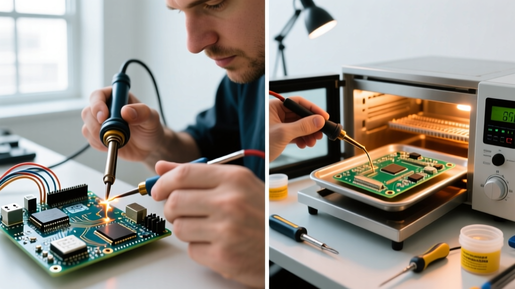
J-STD-001 strictly governs thermal profiles and tip maintenance. You cannot use uncalibrated, generic soldering stations.
- Soldering Stations: Facilities must upgrade to closed-loop, digitally calibrated stations like the JBC CD-2BQF or Hakko FX-951. These units log thermal data and prevent operators from overriding maximum temperature limits (typically 350°C for lead-free SAC305). Budget $600 to $900 per station.
- Inspection Optics: Visual inspection of 0402 and 0201 components requires high-end digital microscopes. Systems like the Vision Engineering Mantis or digital AOI (Automated Optical Inspection) rigs from Omron are necessary to verify the mandatory <90-degree wetting angles and detect micro-cracking.
- Flux Management: The standard dictates strict cleanliness protocols. You may need to invest in ROSE (Resistivity of Solvent Extract) or SIR (Surface Insulation Resistance) testing equipment if your OEM requires ionic contamination verification.
Flux Residue and Cleanliness Standards
One of the most heavily audited sections of J-STD-001 revolves around flux residues. The standard classifies fluxes by type (e.g., ROL0, ROH1) and mandates specific cleaning protocols based on the classification. For 'No-Clean' fluxes (ROL0), the standard permits leaving the residue on the board only if the manufacturer can prove it does not cause electrochemical migration (ECM) or interfere with conformal coating adhesion. In 2026, with the widespread use of low-VOC, halogen-free fluxes, improper curing of no-clean residues under BGA components remains a leading cause of field failures. If you cannot guarantee complete flux activation and curing via precise reflow profiles, J-STD-001 mandates an aqueous or solvent cleaning process.
Step-by-Step Implementation Framework
If the decision matrix dictates that your organization requires formal compliance, follow this phased implementation strategy:
- Gap Analysis (Weeks 1-2): Audit your current work instructions against the latest revision of the IPC's official J-STD-001 documentation. Identify deviations in PTH barrel fill, SMT fillet sizing, and wire preparation.
- Tooling Calibration (Weeks 3-4): Implement a digital calibration schedule for all thermal profiling equipment, solder baths, and reflow ovens. Establish a tip-change log for hand soldering stations to prevent copper dissolution and thermal lag.
- Core Team CIT Training (Weeks 5-6): Send your lead process engineers to CIT training. They will become the internal authority for interpreting the standard's nuances.
- Operator CIS Rollout (Weeks 7-12): Train line operators in cohorts. Utilize hands-on labs focusing on your specific product mix (e.g., heavy copper power boards vs. HDI telecom boards).
- Mock Audit and AOI Programming (Weeks 13-16): Program your AOI machines with J-STD-001 defect libraries. Conduct a mock audit using an external consultant from an organization like BEST Inc. to identify blind spots before your official OEM audits.
Common Audit Failure Modes and Edge Cases
Even facilities with certified operators frequently fail initial OEM audits due to misinterpretations of the standard. Be vigilant against these specific edge cases:
Edge Case 1: The 'Shiny vs. Dull' Solder Myth
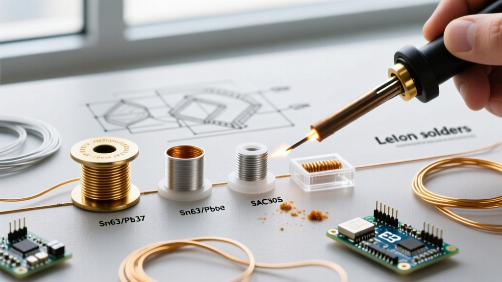
Expert Insight: A massive point of failure in Class 2 and Class 3 inspections is the visual rejection of perfectly good lead-free solder joints. Operators trained on legacy Sn63/Pb37 (leaded) solder expect a bright, shiny fillet. However, lead-free alloys like SAC305 (Tin/Silver/Copper) naturally cool with a dull, grainy, or matte finish. J-STD-001 explicitly states that a dull or grainy appearance in lead-free solder is an acceptable process condition, not a defect, provided the wetting and contour criteria are met. Over-rejecting these joints destroys yield and profitability.
Edge Case 2: Solder Mask Damage and Conformance
During hand soldering of heavy PTH connectors, operators often dwell the iron too long, causing the solder mask to blister or lift. While a minor scratch might pass an internal SOP, J-STD-001 Class 3 strictly prohibits solder mask blistering that exposes underlying copper traces, as this creates a pathway for dendritic growth and short circuits in humid environments. Implementing strict maximum dwell times (e.g., 3 seconds per joint) and using high-thermal-capacity tips like the JBC C245 series is mandatory to prevent this.
Edge Case 3: Wire Tinning and Solder Wicking
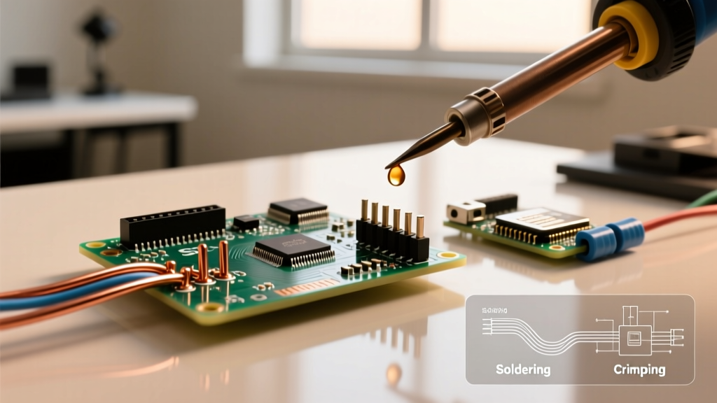
For wire-to-board assemblies, J-STD-001 dictates that solder must not wick up the wire beyond the insulation gap or into the mating area of a connector. A common failure mode occurs when operators pre-tin wires excessively, causing the solder to creep under the insulation, making the wire rigid and prone to snap under vibration. Using precise strip lengths and controlled dip-tinning pots with active flux skimming is required to pass this criterion.
Final Verdict: Is J-STD-001 Right for You?
If you are manufacturing consumer gadgets with a planned obsolescence of two years, the $20,000+ investment in J-STD-001 certification and equipment upgrades will likely not yield a positive ROI. Stick to rigorous internal SOPs and IPC-A-610 visual training. However, if your 2026 roadmap includes pivoting into automotive, medical, or industrial IoT sectors, J-STD-001 compliance is not optional—it is the foundational tollbooth to enterprise supply chains. By treating the standard as a process engineering framework rather than a mere inspection checklist, you transform soldering from a manual variable into a predictable, high-yield science.