
The Genesis of Capillary Action
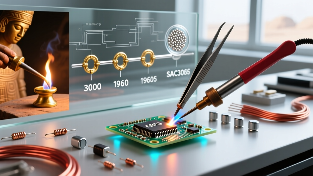
Long before the first printed circuit board (PCB) was etched, ancient Mesopotamian goldsmiths were utilizing the fundamental principles of joint soldering to fuse precious metals. The core mechanism—using a filler metal with a lower melting point than the base metals, drawn into a gap via capillary action—remains unchanged. However, the metallurgy, thermal delivery systems, and reliability standards governing joint soldering have undergone radical transformations. Understanding this evolution is not merely an academic exercise; for modern electronics manufacturers and DIY engineers in 2026, historical context dictates how we select soldering stations, flux chemistries, and inspection criteria today.
Chronological Milestones in Joint Formation
The trajectory of joint soldering can be mapped through distinct metallurgical and technological eras. The table below outlines the critical shifts that brought us to modern electronics assembly.
| Era | Primary Alloy / Tech | Melting Point | Key Innovation & Application |
|---|---|---|---|
| 4000 BC - 1800s | Gold-Tin, Lead-Tin | Varies (183°C - 300°C+) | Blowpipe heating; jewelry, stained glass, and early plumbing joints. |
| 1910s - 1950s | Sn60/Pb40 | 183°C - 190°C | Invention of the electric soldering iron; mass production of radio tubes. |
| 1960s - 1990s | Sn63/Pb37 (Eutectic) | 183°C (Exact) | Wave soldering and Curie-point temperature control; the PCB revolution. |
| 2006 - 2015 | SAC305 (Lead-Free) | 217°C - 220°C | RoHS compliance; shift to higher thermal mass equipment and nitrogen atmospheres. |
| 2020s - 2026 | SnBiAg, Laser Reflow | 138°C - 217°C | Closed-loop laser joint soldering; low-temp alloys for heat-sensitive micro-BGAs. |
The Metallurgical Revolution: From Eutectic to SAC305
For over a century, the undisputed king of joint soldering in electronics was Sn63/Pb37 (63% Tin, 37% Lead). This specific ratio is eutectic, meaning it transitions directly from solid to liquid at a single temperature (183°C) without passing through a plastic (semi-solid) phase. This eliminated the risk of 'cold joints' caused by component movement during the cooling phase.
The paradigm shifted dramatically with the enforcement of the EU RoHS Directive, which restricted lead in consumer electronics. The industry standardized on SAC305 (96.5% Sn, 3.0% Ag, 0.5% Cu). While environmentally necessary, SAC305 introduced severe challenges for joint soldering:
- Higher Melting Point: At 217°C–220°C, SAC305 requires significantly more thermal energy, accelerating tip oxidation and degrading flux activators prematurely.
- Pasty Range: Unlike eutectic Sn63/Pb37, SAC alloys have a slight plastic range, demanding stricter profiling in reflow ovens to prevent grainy, disturbed joints.
- Wetting Characteristics: Lead-free alloys exhibit higher surface tension, resulting in poorer wetting and requiring more aggressive no-clean or water-soluble fluxes to achieve acceptable capillary flow.
Expert Insight: A reliable solder joint relies on the formation of an Intermetallic Compound (IMC) layer, typically Cu6Sn5 or Cu3Sn, at the boundary of the copper pad and the solder. An optimal IMC layer is 1 to 3 micrometers thick. Excessive dwell times with modern SAC305 alloys cause the IMC layer to overgrow, resulting in a brittle joint prone to mechanical shear failure under thermal cycling.
Thermal Delivery: Curie Points to Smart Cartridges
The evolution of the soldering iron directly mirrors the demands of changing alloys. In the 1960s, the Weller TCP (Temperature Controlled Pencil) revolutionized joint soldering by utilizing a magnetic Curie point sensor embedded in the tip. When the tip reached its designated temperature, the magnetic core lost its magnetism, breaking the circuit to the heating element. This was a massive leap from the unregulated 'hatchet' irons of the past.
However, the high thermal drain of SAC305 and the dense ground planes of 2026 multi-layer PCBs exposed the limitations of traditional ceramic-heater stations. Modern premium systems, such as the JBC CD-2B or Hakko FX-951, utilize smart cartridge technology. In a JBC C245 cartridge, the heater and the thermocouple are integrated directly into the tip's copper core. This allows the station to detect a temperature drop the millisecond the tip touches a copper pour, delivering a massive burst of power (often 130W+ peak) to recover thermal equilibrium in under 2 seconds. When budgeting for a workstation today, spending $600–$750 on a smart-cartridge system is a direct response to the unforgiving thermal requirements of post-RoHS joint soldering.
The Unintended Consequence: Tin Whiskers and Reliability
The transition to lead-free joint soldering brought an old, forgotten reliability issue back to the forefront: tin whiskers. These are spontaneous, microscopic, crystalline structures of tin that grow from the solder joint or component leads, potentially causing catastrophic short circuits in high-impedance or high-voltage circuits.
According to the NASA NEPP Tin Whisker Database, the addition of even 1-2% lead to tin alloys historically suppressed this phenomenon by altering the crystal lattice stress. With the ban on lead, the industry had to develop new mitigation strategies for joint soldering, including:
- Matte Tin Finishes: Replacing bright tin electroplating (which introduces high compressive stress) with annealed matte tin.
- Conformal Coating: Applying acrylic or urethane coatings (e.g., Humiseal 1B31) to physically block whisker growth from bridging adjacent joints.
- Bismuth Alloying: Adding trace amounts of Bismuth to the SAC alloy to disrupt the tin crystal structure and relieve internal stresses.
2026 Frontiers: Laser and Induction Joint Soldering
As components shrink to 01005 (0.4mm x 0.2mm) passives and micro-BGAs with pitches below 0.3mm, traditional contact-based joint soldering reaches its physical limits. Iron tips simply cannot access these dense geometries without risking pad lifting or collateral thermal damage to adjacent plastic connectors.
This has driven the adoption of Laser Joint Soldering in high-end manufacturing and advanced rework. Systems utilizing 980nm diode lasers (ranging from 50W to 200W) focus a precise beam onto the solder paste or preform. Crucially, modern laser systems employ closed-loop pyrometer feedback. The pyrometer reads the infrared emission of the joint in real-time, dynamically adjusting the laser power to maintain an exact temperature profile (e.g., ramping to 235°C, holding for 1.5 seconds, and cooling at a controlled rate). This ensures perfect IMC formation without any physical contact, eliminating tip wear and cross-contamination entirely.
Buyer's Framework: Applying History to Modern Purchases
When evaluating equipment and materials for joint soldering today, historical context provides a practical decision-making framework:
1. Match the Station to the Alloy
If you are strictly working with legacy Sn63/Pb37 or low-temperature Sn42/Bi58 (138°C) for simple repairs, a $120 entry-level station with a standard ceramic heater is entirely sufficient. However, if your daily workflow involves SAC305 on multi-layer automotive or aerospace boards, you must invest in a direct-drive smart cartridge system to prevent cold joints and pad delamination.
2. Respect the Flux Chemistry
Modern no-clean fluxes are engineered to activate at higher temperatures (200°C+). If you attempt to use a low-wattage iron that fails to push the joint past the flux's activation threshold, you will be left with highly corrosive, unreacted activator residues that will eventually cause electrochemical migration (dendrite growth).
3. Adhere to Evolved Inspection Standards
Visual inspection criteria have tightened significantly. The IPC-A-610 Standard for Class 3 (High-Performance) products dictates strict wetting angles and fillet contours. A joint that was considered 'acceptable' in the 1990s may be classified as a defect today due to the harsher thermal and mechanical environments modern electronics endure.
The evolution of joint soldering is a testament to the electronics industry's ability to adapt to environmental mandates and miniaturization trends. By understanding the metallurgical and thermal history of the craft, engineers and hobbyists can make informed, precise choices that ensure the longevity and reliability of their assemblies in 2026 and beyond.