
The Anatomy of Good Soldering Joints: An Expert Roundup
In the rapidly evolving electronics landscape of 2026, where 0201 metric components and high-density interconnect (HDI) boards are standard, the margin for error in PCB assembly has practically vanished. Whether you are building a custom mechanical keyboard, repairing a vintage amplifier, or prototyping an IoT sensor, achieving good soldering joints is the fundamental baseline for reliability. But what exactly defines a "good" joint? Is it just about shininess?
To answer this, we convened insights from IPC-certified trainers, veteran aerospace electronics engineers, and metallurgy experts. This roundup distills decades of hands-on experience into actionable, precise guidance on thermal profiling, flux chemistry, and tooling selection.
Visual Standards: What the Experts Look For
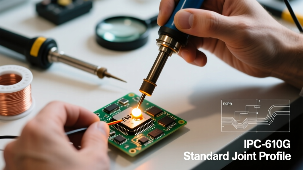
According to the IPC-A-610 standard for electronic assemblies, a good soldering joint is not merely defined by aesthetics, but by specific geometric and metallurgical criteria. The primary indicators are wetting and fillet shape.
IPC Acceptability Matrix for PTH (Plated Through-Hole) Joints
| Criteria | Class 1 (General) | Class 2 (Dedicated Service) | Class 3 (High Performance) |
|---|---|---|---|
| Wetting Angle | Less than 90° | Less than 90° | Ideally 15° - 45° |
| Barrel Fill | Not specified | Minimum 50% vertical fill | Minimum 75% vertical fill |
| Fillet Shape | Acceptable if wetted | Concave to slightly convex | Smooth, continuous concave |
| Surface Texture | Matte or shiny acceptable | Smooth, undisturbed | Smooth, shiny (leaded) or matte (lead-free) |
"A common beginner mistake is equating a shiny joint with a good joint. With modern lead-free SAC305 alloys, a perfectly reliable joint will often have a dull, matte finish. Forcing it to look shiny by tweaking the iron temperature usually results in a burnt flux residue and a brittle intermetallic compound (IMC) layer."
— Sarah Jenkins, IPC Master Specialist & Aerospace Soldering Trainer
Thermal Profiling: Beyond the Dial Setting
The most frequent point of failure in creating good soldering joints is improper thermal management. Experts emphasize that heat transfer matters far more than the temperature setting on your soldering station.
Alloy-Specific Temperature Targets
Different alloys require distinct thermal profiles. Here is the consensus from industry professionals for hand soldering:
- Sn63/Pb37 (Eutectic Leaded): Melts at 183°C (361°F). Experts recommend an iron tip temperature of 300°C to 320°C. Because it is eutectic, it transitions instantly from liquid to solid, minimizing the risk of disturbed joints.
- SAC305 (Lead-Free): Melts between 217°C and 220°C (422°F - 428°F). Requires a higher tip temperature of 350°C to 380°C. SAC305 has a "pasty" phase range; if the component moves during this cooling window, the joint will suffer from micro-fractures.
- Sn96.5/Ag3.0/Cu0.5 with Nickel Doping: Increasingly popular in 2026 for high-reliability automotive boards. Requires precise thermal soaking to prevent copper pad dewetting.
According to guidelines referenced in the NASA Workmanship Standards (NASA-STD-8739.3), the dwell time—the total time the iron is in contact with the joint—should ideally not exceed 2 to 3 seconds for standard surface mount devices (SMDs) to prevent delamination of the PCB substrate.
Flux Chemistry: The Unsung Hero
You cannot achieve good soldering joints without the correct flux. Flux removes oxidation from the copper pads and component leads, allowing the molten solder to "wet" the surfaces and form a strong Intermetallic Compound (IMC).
Expert Flux Recommendations by Application
- General Purpose / Prototyping (Rosin): Kester 44 or MG Chemicals 8350A. These RMA (Rosin Mildly Activated) fluxes are incredibly forgiving, provide excellent wetting, and leave a hard, protective residue. Cost: ~$25 for a 100g spool of flux-core wire.
- Production / No-Clean (ROL0/ROL1): Kester 245 or Indium Corporation CW-807. Designed for environments where post-solder cleaning is impossible. The residue is non-conductive and non-corrosive. Cost: ~$35-$45 per spool.
- Repair / Rework (Water-Soluble): Chip Quik SMD291AX. Highly active organic acid (OA) fluxes that cut through heavy oxidation on old boards. Warning: Must be cleaned with distilled water or PCB cleaner immediately after soldering to prevent galvanic corrosion.
Tooling: Selecting the Right Tip Geometry
Ask any master technician about their biggest pet peeve, and they will likely point to the conical (pencil) tip. "Conical tips are a trap," notes David Aris, a senior rework engineer. "They have terrible thermal mass transfer because only the very point of the tip contacts the pad. You end up pressing harder, damaging the pad, and creating cold joints."
The Expert Tip Selection Guide
To consistently produce good soldering joints, match the tip geometry to the thermal mass of the component:
- Chisel Tips (e.g., Weller RT3, Hakko T18-D16): The gold standard for 80% of tasks. The flat face maximizes surface area contact, ensuring rapid heat transfer into the pad and lead. Ideal for 0603 to 0805 SMDs and standard DIP ICs.
- Bevel / Hoof Tips (e.g., Weller RT4B, Hakko T18-C3): Excellent for drag soldering SOIC and QFP surface-mount ICs. The concave scoop holds a small reservoir of molten solder and flux, smoothing out bridges as you pull across the pins.
- Heavy-Duty Blade / Spade (e.g., Weller RT8, Hakko T18-D32): Essential for grounding lugs, thick motor wires, and large electrolytic capacitor leads. The massive thermal mass prevents the soldering iron from "bogging down" when touching high-heat-sink areas.
Troubleshooting: Diagnosing the "Bad" Joint
Even experts make mistakes. Recognizing failure modes is critical for rework. Here is how to identify and fix the most common joint defects:
1. The Cold Joint
Appearance: Lumpy, dull, and irregularly shaped. Often looks like a blob sitting on top of the pad rather than flowing into it.
Cause: Insufficient heat applied to the component lead, or removing the iron before the flux has fully activated and the solder has flowed.
The Fix: Apply fresh liquid flux. Reheat the joint simultaneously on the pad and the lead until the solder flashes and flows smoothly.
2. The Disturbed Joint
Appearance: Frosty, crystalline, or cracked appearance. Common with lead-free SAC305.
Cause: The component or wire moved while the solder was in its semi-solid "pasty" cooling phase.
The Fix: Flux and reflow. Hold the component absolutely still with tweezers until the solder completely solidifies (usually 1.5 to 2 seconds).
3. Dewetting and Non-Wetting
Appearance: Solder balls up and pulls away from the edges of the pad, exposing bare copper or base metal (dewetting), or refuses to stick to the pad entirely (non-wetting).
Cause: Severe oxidation on the PCB pad, contaminated surfaces, or an expired/ineffective flux core.
The Fix: For non-wetting, scrape the pad gently with a fiberglass pen, apply aggressive water-soluble flux, and use a slightly wider chisel tip to deliver more thermal energy.
Final Takeaways from the Experts
Achieving good soldering joints is not about buying the most expensive $500 soldering station; it is about understanding the metallurgy and physics at play. By respecting the specific thermal requirements of your chosen alloy, utilizing the correct flux chemistry for your environment, and abandoning conical tips in favor of high-surface-area chisels, you will elevate your assembly reliability to IPC Class 3 standards. Remember: let the flux do the cleaning, let the tip geometry do the heating, and let the solder flow naturally.