
The Critical Role of Solderability Screening in Modern Manufacturing
In high-reliability electronics manufacturing, discovering poor component solderability during the mass reflow or wave soldering process is a catastrophic and expensive failure mode. Defects like tombstoning, non-wetting, de-wetting, and head-in-pillow (HiP) often trace back to degraded component finishes or contaminated PCB pads. This is where solderability screening becomes an indispensable gatekeeping process. By testing a statistical sample of components and bare boards before they hit the SMT line, manufacturers can predict assembly yield and reject compromised batches.
However, not all screening methods are created equal. The IPC standards body outlines several distinct testing methodologies, each suited for different component geometries, metallizations, and production environments. In this comprehensive comparison, we break down the three primary solderability screening methods—Dip and Look, Solder Globule, and Wetting Balance—to help you select the right protocol and equipment for your 2026 production floor.
Core Solderability Screening Methods Compared
1. Dip and Look (The Industry Workhorse)
The Dip and Look test is the most widely adopted qualitative screening method, heavily referenced in IPC J-STD-002 and NASA workmanship standards. It is designed to simulate wave soldering or manual hand soldering conditions.
- Procedure: Component leads are dipped into a mildly activated rosin flux (typically ROL0 or RMA types like Kester 185 or Alpha NR310), air-dried, and then immersed into a static solder bath.
- Parameters: For lead-free SAC305 alloys, the bath temperature is strictly maintained at 245°C ± 5°C. Immersion depth is usually 2mm to 4mm, with an immersion speed of roughly 25 mm/s. Dwell time is typically 3 to 5 seconds.
- Evaluation: The component is removed, cleaned, and inspected under 10x to 30x magnification. The acceptance criteria generally require a minimum of 95% continuous solder coverage on the immersed surfaces, with no evidence of de-wetting (where solder retracts and forms droplets) or non-wetting (where the base metal remains exposed).
Best For: Through-hole components, large SMD terminations, and PCB edge connectors. It is fast, relatively inexpensive, and provides an immediate visual go/no-go result.
2. Solder Globule Test (For Micro-SMDs)
When dealing with micro-BGAs, 0201 chip components, or fine-pitch QFNs, the standard Dip and Look method is entirely impractical. The surface tension of a bulk solder bath will obscure the tiny terminations. Enter the Solder Globule test.
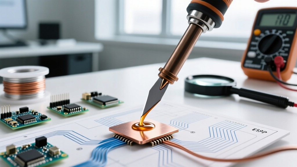
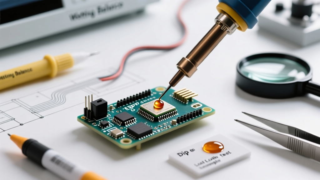
- Procedure: A tiny, pre-weighed sphere of solder (ranging from 0.5mm to 2.0mm in diameter) is placed on a heated, flux-coated copper block or directly onto the component termination using Teflon-coated tweezers.
- Parameters: The heat source melts the globule. The time it takes for the molten solder to completely wet and envelop the component termination is measured with a stopwatch or high-speed camera.
- Evaluation: A pass requires the globule to wet the termination within a specified timeframe (usually under 2.0 seconds for SAC alloys) and exhibit a smooth, concave fillet without splitting.
Best For: Surface mount terminations where bulk immersion would cause solder bridging or obscure visual inspection. It is highly effective for verifying the solderability of bottom-terminated components (BTCs).
3. Wetting Balance Testing (The Quantitative Standard)
While Dip and Look is qualitative (relying on human visual inspection), the Wetting Balance test provides hard, quantitative data. It measures the actual forces of wetting and buoyancy over time.
- Procedure: The component lead is suspended from a highly sensitive force transducer and immersed into a molten solder bath. As the solder wets the lead, it pulls the lead downward (wetting force). The buoyancy of the displaced solder pushes it upward.
- Parameters: The equipment plots a meniscus graph (Force vs. Time). Key metrics include the time to cross the zero-force line (time to wet) and the maximum wetting force achieved.
- Evaluation: According to Surface Mount Technology Association (SMTA) guidelines, a highly solderable lead will cross the zero line in under 1.0 second and reach a high maximum wetting force, indicating excellent metallurgical bonding.
Best For: Incoming quality control (IQC) labs requiring statistical process control (SPC) data, root-cause analysis of field failures, and evaluating new alloy flux combinations.
Method Comparison Matrix
| Screening Method | Metric Type | Ideal Component Type | Standard Reference | Equipment Cost (Est.) |
|---|---|---|---|---|
| Dip and Look | Qualitative (Visual) | Through-hole, Large SMDs | IPC J-STD-002 | $2,500 - $5,000 |
| Solder Globule | Time-based (Stopwatch) | 0201 Chips, Micro-BGAs, QFNs | IPC J-STD-002 | $3,000 - $6,000 |
| Wetting Balance | Quantitative (Force/Time) | All (Lab/Root Cause Analysis) | IPC J-STD-003 / ISO 9455 | $15,000 - $28,000 |
Accelerated Aging: The Missing Link in Screening
A common mistake in solderability screening is testing components straight out of the vacuum-sealed MSL (Moisture Sensitivity Level) bag. This only proves they are solderable today. To predict shelf-life viability, screening must incorporate accelerated aging.
Pro-Tip: Steam aging is the industry standard for simulating warehouse shelf life. Exposing components to 100°C steam for 8 hours is widely accepted as equivalent to 6 to 12 months of ambient warehouse storage, rapidly oxidizing poor-quality finishes like thin Immersion Silver (IAg) or degraded ENIG.
If a batch of ENIG (Electroless Nickel Immersion Gold) PCBs passes Dip and Look fresh but fails after 8 hours of steam aging, you have successfully intercepted a batch prone to 'Black Pad Syndrome' or severe oxidation before it ruins your assembly yield.
The 2026 Equipment Buyer's Reality: Costs and Consumables
Setting up an in-house solderability screening lab requires more than just buying the bath. The shift toward complex lead-free alloys (like SAC305, SAC405, and low-temperature SN100C) has changed the operational economics.
- Solder Baths: A high-quality, digitally controlled static solder bath (e.g., from PACE or OK International) costs between $2,500 and $5,000. However, lead-free baths generate massive amounts of dross (oxidized solder scum).
- Nitrogen Blanketing: To mitigate dross formation and maintain consistent wetting in SAC305 baths, modern labs use nitrogen generators. Budget an additional $8,000 to $12,000 for a localized N2 blanket system, plus roughly $300/month in maintenance.
- Wetting Balances: Precision instruments like the Malcom ST-1 or the Ni100C wetting balance represent a major CapEx investment ($18,000+). They require strict calibration using certified reference coupons and specialized software licenses.
- Consumables: High-purity fluxes, isopropyl alcohol (IPA) for cleaning, and certified solder spheres for globule testing will run a mid-volume lab about $400 to $600 per month.
Edge Cases: When Screening Fails to Predict Assembly Yield
Even rigorous solderability screening has blind spots. Understanding these edge cases is what separates novice technicians from senior process engineers.
1. Thermal Mass and Reflow Profiling
A heavy copper power inductor might pass the Dip and Look test flawlessly because it sits in the 245°C bath for 5 full seconds. However, on the SMT line, the component's massive thermal mass might prevent its terminations from reaching the 217°C liquidus temperature during a standard 60-second reflow peak, resulting in a cold solder joint. Screening tests do not simulate the thermal dynamics of a reflow oven.
2. Palladium-Nickel (PdNi) Finishes
Components with thick PdNi finishes (often used in automotive and aerospace for whisker mitigation) can exhibit delayed wetting. They may fail the strict 2-second time-to-wet criteria in a wetting balance test, yet still form perfectly reliable intermetallic compounds (IMCs) during a prolonged reflow profile. Strict adherence to screening thresholds can lead to the false rejection of perfectly good aerospace-grade components.
FAQ: Solderability Screening Best Practices
How often should we perform solderability screening on incoming components?
For commercial-grade products, screening is typically done on a per-lot basis upon receiving (IQC). For high-reliability (Class 3) medical or aerospace assemblies, screening should be performed on every reel or tray, especially if the date codes indicate the components have been in storage for more than 12 months.
Can we use our wave soldering machine for Dip and Look testing?
Technically, you can dip a component into the wave pot, but it is highly discouraged. Wave pots contain dissolved copper and other contaminants from previous PCB assemblies. Screening requires a pristine, dedicated static bath with strictly controlled alloy composition to ensure the test results reflect the component's finish, not the contamination of your production solder.
What is the most common cause of sudden screening failures?
Improper storage. Components stored in environments with high humidity and fluctuating temperatures without desiccant or moisture barrier bags (MBBs) will rapidly oxidize. Always cross-reference screening failures with the manufacturer's date code (D/C) and the storage conditions of your inventory room.