
The Stakes of Industrial Soldering Quality Assurance
In hobbyist electronics, a magnifying glass and a multimeter are usually sufficient to verify a circuit. In industrial manufacturing—spanning aerospace, automotive (AEC-Q100), and life-saving medical devices—a single compromised solder joint can lead to catastrophic system failure, massive recall costs, and severe liability. As of 2026, the miniaturization of components down to the 01005 imperial footprint (0.4mm x 0.2mm) and the widespread adoption of high-density interconnect (HDI) boards have rendered manual visual inspection entirely obsolete. Today, a robust soldering test protocol requires a multi-tiered, automated approach governed by stringent international standards.
For Electronics Manufacturing Services (EMS) providers and original equipment manufacturers (OEMs), understanding the hierarchy of soldering test methods is critical for balancing throughput, cost, and defect detection. This guide details the industry-standard testing frameworks, non-destructive and destructive analysis techniques, and the specific IPC criteria that define a pass/fail solder joint in high-reliability environments.
Core IPC Standards Governing Soldering Tests
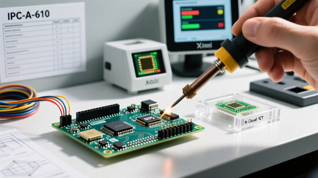
Before deploying any inspection hardware, QA engineers must establish the acceptance criteria. The electronics industry relies heavily on the IPC (Association Connecting Electronics Industries) standards to define what constitutes a reliable solder joint. According to the IPC-A-610 Acceptability of Electronic Assemblies standard, assemblies are categorized into three distinct classes:
- Class 1 (General Electronic Products): Focuses on basic functionality. Solder joints need only be electrically conductive and mechanically stable enough for benign environments. Example: Consumer toys, basic lighting.
- Class 2 (Dedicated Service Electronic Products): Requires extended life and sustained performance, though uninterrupted service is not critical. Example: Commercial laptops, telecommunications routers.
- Class 3 (High-Performance Electronic Products): Demands continuous, on-demand performance with zero downtime tolerance. Solder joints must withstand extreme thermal, mechanical, and vibrational stress. Example: Aerospace flight controls, implantable medical devices, automotive braking systems.
For through-hole technology (THT), a Class 2 soldering test requires a minimum 50% barrel fill in plated through-holes (PTH), whereas a Class 3 test mandates a 75% minimum barrel fill, with specific wetting angles on the solder fillet. Furthermore, the SMTA Knowledge Base and IPC J-STD-001 provide the foundational requirements for soldered electrical and electronic assemblies, dictating everything from flux activity levels to the acceptable limits of solder voiding in surface-mount pads.
Primary Non-Destructive Soldering Test Methods
Modern production lines utilize a sequence of automated systems to catch defects at the earliest possible stage, preventing compounding rework costs.
1. Automated Optical Inspection (AOI)
AOI is the frontline soldering test for surface-mount technology (SMT) assemblies. Modern 3D AOI systems, such as the Koh Young Zenith or Omron VT-S1080, utilize structured light projection and multi-angle cameras to measure solder paste volume, component coplanarity, and fillet height with 10-micron resolution. In 2026, AI-driven defect recognition algorithms have drastically reduced false-call rates (pseudo-defects), which historically plagued 2D AOI systems when dealing with reflective solder alloys or complex PCB topographies.
2. Automated X-Ray Inspection (AXI)
AOI cannot see beneath the component body. For Bottom Termination Components (BTCs) like Quad Flat No-leads (QFNs) and Ball Grid Arrays (BGAs), X-ray inspection is mandatory. IPC-7095 specifies that BGA solder voiding must not exceed 25% of the total joint area for standard applications, and often less for high-power RF applications due to thermal dissipation requirements. 3D Computed Tomography (CT) X-ray systems can now slice through a BGA joint digitally, identifying micro-cracks, head-in-pillow (HiP) defects, and solder bridging that 2D X-ray might obscure due to component overlap.
3. In-Circuit Testing (ICT) and Flying Probe
While AOI and AXI verify the physical geometry of the solder joint, ICT verifies the electrical integrity. ICT utilizes a custom bed-of-nails fixture to make contact with test pads on the PCB, applying specific voltages and measuring resistance, capacitance, and inductance. This soldering test catches electrically open joints (cold solder) or short circuits caused by microscopic solder bridging. For high-mix, low-volume production, Flying Probe testers (e.g., Takaya APT-1400F) use robotic arms to test nodes sequentially, eliminating the $15,000–$40,000 tooling cost of a bed-of-nails fixture.
4. Boundary Scan (JTAG)
For highly complex digital boards where physical test access is limited by dense routing, Boundary Scan testing per the IEEE 1149.1 Standard allows QA engineers to test solder joints on BGA and fine-pitch QFP components purely through software. By shifting test vectors through the boundary-scan cells embedded in the silicon die, engineers can verify the continuity of every single pin without requiring physical probe access.
Destructive vs. Non-Destructive Soldering Test Matrix
Choosing the right soldering test depends on production volume, product class, and budget. The matrix below outlines the primary methods utilized in industrial QA.
| Test Method | Type | Primary Target Defect | Equipment Cost Range (USD) | Throughput Impact |
|---|---|---|---|---|
| 3D AOI | Non-Destructive | Tombstoning, insufficient solder, skew | $80,000 - $180,000 | Low (Inline) |
| 2D/3D AXI | Non-Destructive | BGA voiding, hidden shorts, HiP | $120,000 - $350,000+ | Medium (Inline/Offline) |
| Bed-of-Nails ICT | Non-Destructive | Electrical opens, wrong component value | $40,000 - $90,000 (incl. fixture) | Low (High parallel test) |
| Microsectioning | Destructive | IMC layer thickness, barrel cracks | $15,000 - $40,000 (Lab setup) | N/A (Offline sampling) |
| Thermal Shock | Destructive | Fatigue cracking, CTE mismatch failure | $30,000 - $75,000 (Chamber) | N/A (Offline sampling) |
Environmental and Reliability Soldering Tests
For Class 3 aerospace and automotive applications, non-destructive inline testing is only half the battle. QA labs must perform rigorous destructive and environmental soldering tests on sample coupons to validate the long-term metallurgical integrity of the assembly.
Microsectioning (Cross-Sectional Analysis)
Defined by IPC-TM-650 Method 2.1.1, microsectioning involves encasing a PCB sample in epoxy resin, slicing it precisely through the center of a PTH or SMT joint, and polishing it to a mirror finish. The sample is then chemically etched (often using potassium ferricyanide) and examined under a metallurgical microscope. The critical metric here is the Intermetallic Compound (IMC) layer thickness. An ideal IMC layer (typically Cu6Sn5 or Ni3Sn4) should be between 1 to 3 micrometers. If the reflow profile was too hot or the soldering iron dwell time too long, the IMC layer can exceed 5µm, resulting in a highly brittle joint prone to mechanical fracture under vibration.
Thermal Cycling and Shock Testing
Solder joints are subjected to extreme temperature differentials due to the Coefficient of Thermal Expansion (CTE) mismatch between the silicon die, the FR-4 substrate, and the solder alloy itself. Thermal cycling tests (typically -40°C to +125°C for automotive, or -55°C to +125°C for aerospace) force the solder joint to absorb mechanical strain. Lead-free SAC305 (Sn96.5/Ag3.0/Cu0.5) alloys are particularly susceptible to fatigue cracking in large ceramic BGA components during these cycles, often necessitating the use of underfill epoxies to distribute the stress.
Solderability Testing (Dip and Look)
Before components are even placed on the board, incoming QA must verify the solderability of component leads and bare PCB pads. Per IPC J-STD-003, the 'Dip and Look' test involves immersing the lead into a rosin-based flux, followed by a dip into a molten solder pot (typically at 245°C for SnPb or 255°C for SAC305). The meniscus must wet the surface uniformly within 2 seconds, proving that oxidation has not compromised the component's termination finish.
Implementing a Modern Soldering Test Pipeline
To achieve Six Sigma quality levels (3.4 defects per million opportunities), mid-to-high volume EMS providers must implement a sequential testing pipeline. Skipping a step creates blind spots that downstream tests cannot reliably catch.
- Solder Paste Inspection (SPI): A 3D laser scan of the solder paste deposition immediately after the stencil printer. Catches 70% of all SMT defects (bridging, insufficient paste) before components are even placed.
- Pre-Reflow AOI: Verifies component presence, polarity, and alignment before the board enters the reflow oven.
- Post-Reflow 3D AOI: Inspects the final solder fillet geometry, checking for tombstoning, solder balls, and wetting issues.
- AXI Sampling: 100% inspection for BGAs and critical QFNs; statistical sampling for standard passive components.
- ICT / Flying Probe: Validates the electrical continuity and component values, ensuring no internal damage occurred during reflow.
- Functional Test (FCT): The assembled board is powered on and subjected to simulated real-world operating conditions to verify firmware and hardware integration.
Common Failure Modes Detected by Advanced Testing
Understanding what you are looking for is as important as the equipment used. Modern soldering test protocols specifically target these high-risk failure modes:
- Head-in-Pillow (HiP): A BGA defect where the solder paste on the PCB pad and the solder ball on the component reflow, but fail to coalesce into a single homogenous joint, leaving a microscopic gap. Detectable only via high-resolution 3D X-ray or Boundary Scan.
- Tombstoning (Drawbridging): A passive component stands on one end due to uneven wetting forces during reflow. Easily caught by 2D or 3D AOI.
- Electrochemical Migration (ECM): Dendritic growth of metal ions between closely spaced traces under voltage bias, exacerbated by flux residue and humidity. Requires SIR (Surface Insulation Resistance) testing per IPC-TM-650 2.6.3.3.
- Tin Whiskers: Spontaneous crystalline growth of tin from pure tin-plated finishes, capable of causing short circuits years after deployment. Mitigated by using matte tin finishes or conformal coatings.
Conclusion
A comprehensive soldering test strategy is not merely a regulatory hurdle; it is a critical determinant of product lifecycle and brand reputation. By aligning inspection hardware—such as 3D AOI and CT X-ray—with the rigorous acceptance criteria of IPC-A-610 and J-STD-001, manufacturers can transition from reactive defect sorting to proactive process control. As component densities continue to push the physical limits of PCB real estate, investing in automated, data-driven soldering test methodologies remains the most effective insurance policy against field failures.