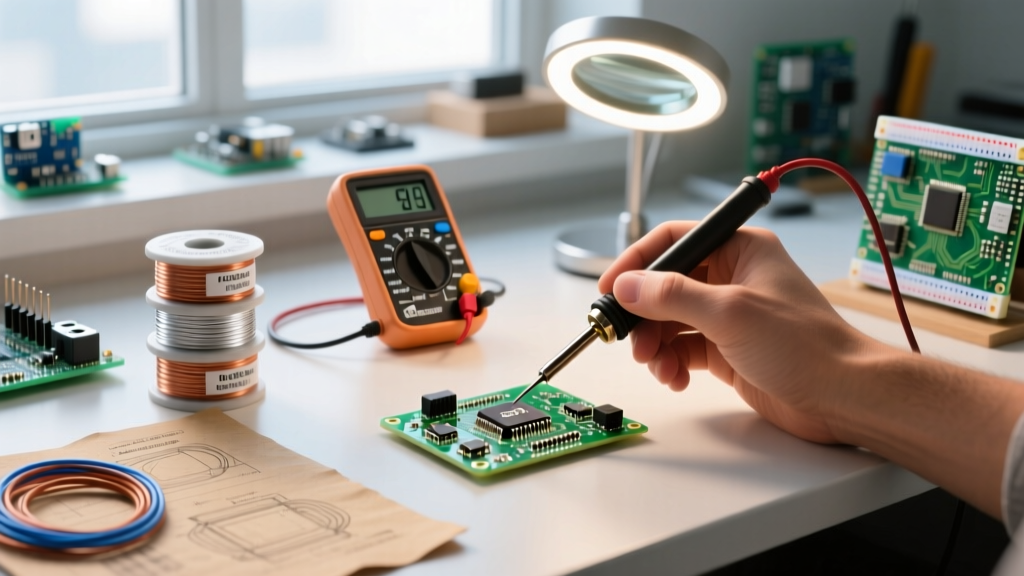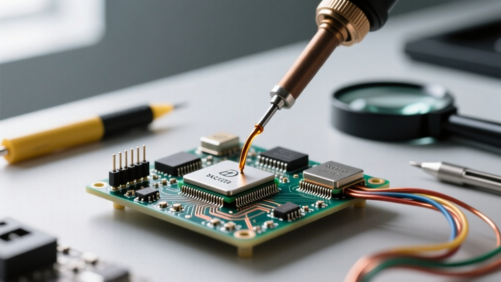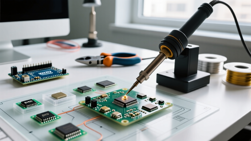

The Dawn of Miniaturization: Beyond Through-Hole
For decades, through-hole technology (THT) dominated electronics manufacturing. Components with long wire leads were inserted into drilled holes on printed circuit boards (PCBs) and secured via wave soldering. While mechanically robust, THT imposed severe limits on component density and routing complexity on the bottom layer of a board. The paradigm shift toward soldering surface mount components did not happen overnight; it was a multi-decade evolution driven by aerospace weight constraints, consumer demand for portability, and radical advancements in metallurgy.
1960s–1980s: NASA, IBM, and the Birth of SMDs
The earliest practical applications of surface mount technology (SMT) were born out of necessity in the aerospace sector. According to NASA's historical archives, the Apollo Guidance Computer (AGC) utilized early iterations of surface-mounted integrated circuits to minimize weight and volume—critical factors for lunar missions. These early 'flat packs' were soldered directly to the PCB pads, eliminating the need for drilled holes and significantly reducing the board's overall mass.
By the 1970s and 1980s, IBM and other computing giants began adopting SMT for hybrid circuits and memory modules. However, the soldering process was largely confined to expensive, vapor-phase reflow systems and rudimentary hot-plate methods. The solder alloys of the era were predominantly tin-lead (Sn63/Pb37), prized for their low eutectic melting point of 183°C and excellent wetting characteristics. For early DIYers and hobbyists, soldering surface mount components by hand was nearly impossible due to the lack of precision temperature-controlled irons and magnification optics.
1990s–2000s: The Consumer Boom and the RoHS Mandate
The 1990s saw SMT explode into consumer electronics. The demand for smaller mobile phones, pagers, and portable CD players forced manufacturers to shrink passive components from 1206 (3.2 x 1.6 mm) down to 0603 (1.6 x 0.8 mm). Automated pick-and-place machines paired with infrared and convection reflow ovens made mass production highly efficient.
A massive metallurgical shift occurred in the mid-2000s. The European Commission's RoHS Directive mandated the removal of lead from consumer electronics. This forced the industry to adopt lead-free alloys, primarily SAC305 (96.5% Tin, 3.0% Silver, 0.5% Copper). SAC305 melts at a higher 217°C and requires peak reflow temperatures up to 245°C. This transition introduced new failure modes, such as tin whiskers and pad cratering, and forced DIYers to upgrade their soldering stations to handle higher thermal recovery demands.
'The transition to lead-free SMT was the single greatest thermal shock to the electronics manufacturing industry, fundamentally altering flux chemistry, reflow profiles, and PCB substrate material limits.' — IPC Manufacturing Standards Review
Package Size Evolution: A Data Matrix
As we look at the trajectory of SMDs, the physical footprint has shrunk to near-microscopic levels. The IPC standards body continuously updates guidelines (like IPC-A-610) to address the inspection criteria for these minuscule joints.
| Era | Standard Package | Dimensions (mm) | Primary Soldering Method | DIY Rework Difficulty |
|---|---|---|---|---|
| 1980s | 1206 / SOIC | 3.2 x 1.6 / 1.27mm pitch | Wave / Early Convection | Low (Standard Iron) |
| 1990s | 0805 / TSSOP | 2.0 x 1.25 / 0.65mm pitch | Convection Reflow | Moderate (Fine Tip Iron) |
| 2000s | 0402 / QFN | 1.0 x 0.5 / 0.5mm pitch | Lead-Free Reflow | High (Hot Air + Microscope) |
| 2010s | 0201 / BGA | 0.6 x 0.3 / Grid Array | Nitrogen-Assisted Reflow | Extreme (Stencil + Reflow Oven) |
| 2020s+ | 01005 / 008004 | 0.4 x 0.2 / 0.25 x 0.125 | Laser / Advanced Convection | Lab-Only (Requires AXI/X-Ray) |
2026 Buyer’s Guide: Gear for Modern SMD Rework
Understanding this history is crucial for making informed purchasing decisions today. Soldering surface mount components in a modern DIY or prototyping lab requires gear that can handle high thermal mass boards (like 10-layer motherboards) while delivering surgical precision for 0402 and 0201 passives.
1. Hot Air Rework Stations
Modern SMD rework relies heavily on controlled airflow. The QUICK 861DW ($389) remains the gold standard for advanced hobbyists and repair technicians. Its 1000W power output ensures rapid thermal recovery, which is critical when removing large ground-plane-connected ICs. For higher-budget labs, the Hakko FR-830 ($650) offers superior airflow stability and digital profile programming, allowing you to mimic specific manufacturer reflow curves.
2. Solder Paste and Stencil Chemistry
Hand-soldering 0201 components with a wire is a recipe for bridging. Modern SMT assembly requires solder paste and stencils. Chip Quik SMD291AX10 ($24.99 per 10g syringe) is a Sn63/Pb37 no-clean paste that remains highly popular for DIYers due to its forgiving 183°C melting point and extended tack time (up to 48 hours). For stencils, while laser-cut stainless steel (0.1mm thickness) is standard for production, DIYers increasingly use nano-coated polyimide (Kapton) stencils cut via Silhouette plotters, reducing prototyping costs from $150 down to under $15 per board.
3. Optical Inspection and Thermal Diagnostics
You cannot solder what you cannot see. A basic magnifying glass is insufficient for modern pitch sizes. The AmScope SM-4TZ ($320) trinocular stereo microscope provides the 7x-45x zoom necessary to inspect 0402 solder fillets for proper wetting and IPC compliance. Furthermore, diagnosing hidden BGA (Ball Grid Array) joints without an X-ray machine is possible using thermal imaging. Attaching a FLIR One Pro ($399) to a smartphone allows technicians to power-cycle a board and spot cold BGA joints by identifying localized thermal anomalies or voltage drops in real-time.
Actionable Troubleshooting: Modern Failure Modes
As components have shrunk and alloys have changed, specific failure modes have become prevalent when soldering surface mount components outside of factory-controlled environments:
- Tombstoning: Common on 0402 and 0201 passives. This occurs when one pad reaches reflow temperature before the other, causing the surface tension of the molten solder to pull the component upright. Solution: Use a 'Ramp-to-Spike' thermal profile rather than a 'Ramp-Soak-Spike' profile to ensure both pads heat simultaneously, and verify that your stencil aperture design includes home-plate reductions to limit paste volume on inner pad edges.
- Head-in-Pillow (HiP): A notorious BGA defect where the solder paste on the PCB pad melts, but the solder sphere on the BGA component does not fully collapse, leaving a disconnected 'pillow' joint. Solution: This is almost always a flux exhaustion issue caused by excessive time above liquidus (TAL). Keep your TAL under 60 seconds and ensure you are using a Type 4 or Type 5 solder paste (smaller powder mesh) for fine-pitch BGAs.
- Pad Cratering: The mechanical tearing of the copper pad from the fiberglass substrate, common when using aggressive lead-free alloys on thin PCBs. Solution: Never apply mechanical leverage with tweezers while the solder is in a semi-solid 'plastic' phase. Wait for full liquidus, and use low-temp Sn42/Bi57 (138°C) solder paste to reduce thermal stress on the board.
Conclusion
The history of soldering surface mount components is a testament to the relentless push for miniaturization and efficiency. From the heavy, hand-wired aerospace modules of the 1960s to the microscopic 008004 passives of today, the techniques and tools have evolved drastically. For the modern DIYer, repair technician, or prototyping engineer, success requires more than just a hot iron; it demands an understanding of thermal profiles, metallurgical shifts, and precision optics. By investing in the right reflow equipment, microscopy, and paste chemistry, you can achieve factory-grade SMT yields right on your workbench.