
The Paradigm Shift: From Drilled Holes to Surface Pads
Before the advent of surface mount soldering, the electronics industry was bottlenecked by Through-Hole Technology (THT). Every component required a drilled hole in the printed circuit board (PCB), limiting routing density, increasing manufacturing costs, and adding significant weight. Today, surface mount technology (SMT) dominates over 95% of all commercial PCB assembly. But this transition was not an overnight revolution; it was a decades-long evolution driven by aerospace constraints, consumer miniaturization, and environmental mandates. Understanding this history is critical for modern electronics buyers, lab managers, and DIY engineers selecting the right reflow profiles, stencil thicknesses, and micro-soldering equipment in 2026.
1960s–1970s: Aerospace Origins and the Flat-Pack Era
The earliest iterations of surface mount soldering were born out of necessity in the aerospace and defense sectors. In the 1960s, NASA’s Apollo program required computing hardware that was extraordinarily light and resistant to intense vibration. The Apollo Guidance Computer (AGC) utilized early integrated circuits packaged in flat-packs, which were surface-mounted directly onto the board rather than inserted into sockets or drilled holes.
"By eliminating the leads passing through the board, early SMT prototypes reduced component weight by up to 70% and allowed for double-sided PCB routing, a critical advantage for the confined spaces of spacecraft."
During this era, IBM also pioneered early surface mount processes for their military and mainframe applications. However, the lack of automated pick-and-place machinery and the high cost of early surface mount components (SMDs) kept the technology confined to high-budget government contracts. Soldering was largely done by hand using specialized micro-irons, as reflow ovens had not yet been invented.
1980s–1990s: The Consumer Boom and Reflow Standardization
The 1980s marked the commercialization of surface mount soldering. The introduction of the Small Outline Integrated Circuit (SOIC) and the Plastic Leaded Chip Carrier (PLCC) allowed consumer electronics manufacturers to shrink devices like camcorders, portable radios, and early mobile phones.
This era also saw the standardization of the reflow soldering process. Instead of wave soldering (which struggled with the shadowing effect of dense SMDs), engineers developed stencil printing for solder paste and infrared (IR) reflow ovens. The industry standardized on the Sn63/Pb37 (Tin/Lead) eutectic alloy, which melted cleanly at 183°C (361°F). This low melting point was forgiving on early FR-4 PCB substrates and allowed for wide thermal process windows.
The Miniaturization Timeline: Passive Component Evolution
As surface mount soldering matured, the industry relentlessly shrank passive components. Below is the historical timeline of SMD resistor and capacitor sizes, illustrating the increasing demand for precision soldering tools and thinner stencils.
| Imperial Size | Metric Size | Dimensions (mm) | Decade of Mainstream Adoption | Typical Stencil Thickness (2026) |
|---|---|---|---|---|
| 1206 | 3216 | 3.2 x 1.6 | 1980s | 4.0 mil (0.10mm) |
| 0805 | 2012 | 2.0 x 1.2 | Early 1990s | 4.0 mil (0.10mm) |
| 0603 | 1608 | 1.6 x 0.8 | Late 1990s | 3.0 mil (0.075mm) |
| 0402 | 1005 | 1.0 x 0.5 | 2000s | 3.0 mil (0.075mm) |
| 0201 | 0603 | 0.6 x 0.3 | 2010s | 2.0 mil (0.05mm) |
| 01005 | 0402 | 0.4 x 0.2 | 2020s | 1.5 mil (0.038mm) / Nano-coated |
| 008004 | 0201 | 0.25 x 0.12 | Emerging (2025+) | Laser-cut step-down / Vapor Phase |
2006: The RoHS Mandate and Metallurgical Upheaval
Perhaps the most disruptive event in the history of surface mount soldering was the enforcement of the EU RoHS Directive in 2006, which banned the use of lead in consumer electronics. This forced the industry to abandon the reliable Sn63/Pb37 alloy in favor of lead-free alternatives, primarily SAC305 (Sn96.5/Ag3.0/Cu0.5).
The transition was brutal for manufacturing engineers. SAC305 has a higher melting point of 217°C (423°F), requiring peak reflow temperatures of 245°C to 260°C. This thermal stress caused widespread delamination in older FR-4 boards, prompting a shift to high-Tg (glass transition temperature) laminates. Furthermore, lead-free solder joints are inherently more brittle, leading to the development of IPC-A-610 standard updates to properly classify lead-free solder joint aesthetics, which naturally appear dull and grainy compared to shiny leaded joints.
2010s to 2026: BGAs, CSPs, and Bottom-Termination
The smartphone revolution demanded that silicon packaging shrink even further than the leads would allow. This gave rise to the Ball Grid Array (BGA) and Chip Scale Package (CSP), where the solder joints are completely hidden beneath the component body. Surface mount soldering evolved from a visual inspection process to an X-ray and automated optical inspection (AOI) science.
Simultaneously, Bottom-Termination Components (BTCs) like the Quad Flat No-leads (QFN) package became ubiquitous. QFNs feature a large exposed thermal pad on the bottom for heat dissipation. Soldering these requires precise stencil aperture reduction (often reducing the thermal pad paste coverage to 60-70% using a window-pane pattern) to prevent the component from 'floating' on a pool of molten solder, which causes open circuits on the delicate perimeter leads.
Buyer’s Guide: Equipping a Modern SMT Lab in 2026
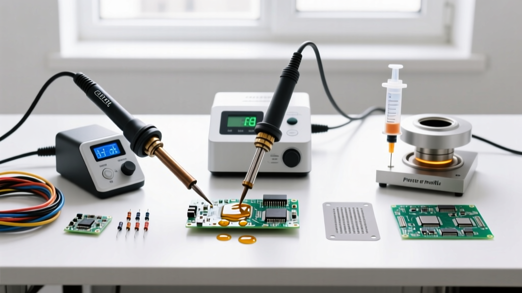
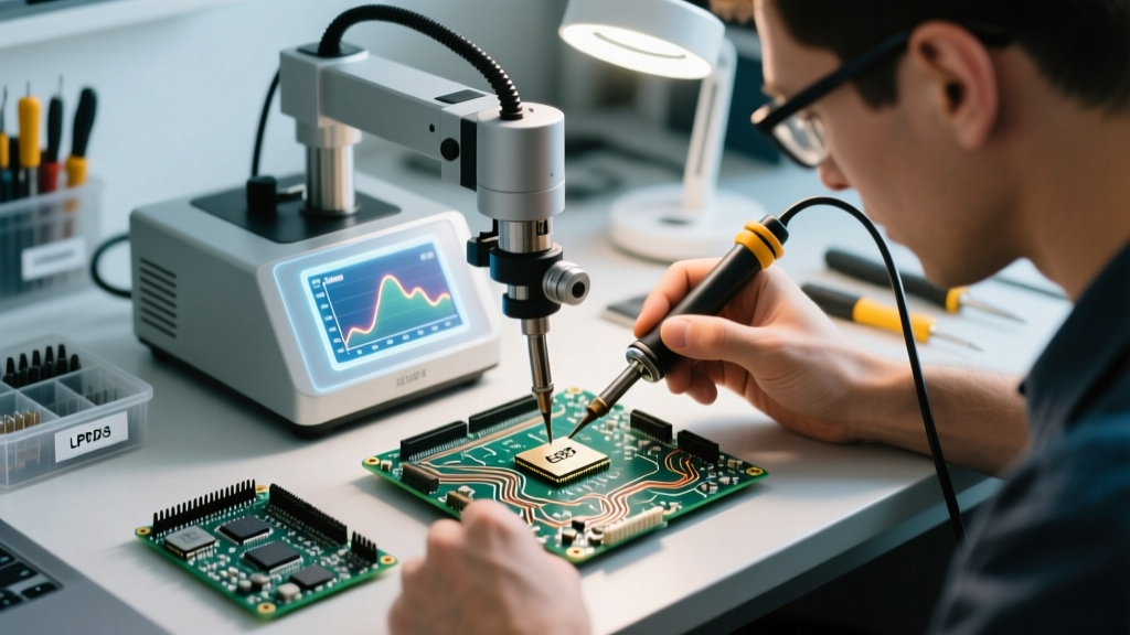
Understanding the historical evolution of SMT directly informs what equipment you need to buy today. If your lab or DIY setup is still relying on 1990s-era through-hole irons, you will instantly destroy modern 0402 components and lift BGA pads. Here is how to align your tooling with modern SMT requirements:
1. Precision Micro-Soldering Stations
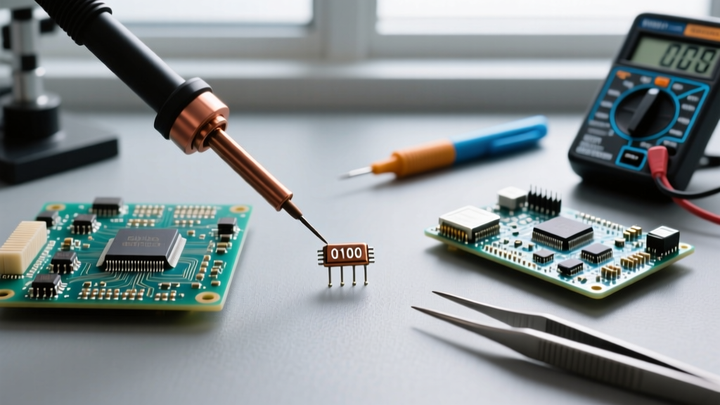
For manual rework of 0201 and 01005 components, thermal recovery and tip mass are critical. You need a station that delivers rapid heat transfer without excessive thermal mass that acts as a heat sink.
- JBC RMVE Nano Soldering Station: Priced around $650, this system uses cartridge-style tips where the heating element is integrated directly into the tip apex. It recovers from 250°C drops in under 2 seconds, making it the gold standard for micro-SMD rework.
- Hakko FX-951: A reliable mid-tier option (~$250) suitable for 0603 and 0402 components, though it struggles with the thermal demands of large QFN ground planes.
2. Advanced Preheating and BGA Rework
Because modern PCBs are dense and act as massive heat sinks, applying top-down heat alone will scorch the board before the BGA solder balls reach 217°C. Bottom preheating is mandatory.
- Hakko FR-830 IR Preheater: At approximately $1,300, this uses targeted infrared to bring the localized PCB area to 130°C–150°C before top-air is applied, preventing thermal shock and pad cratering.
3. Vapor Phase Soldering for Prototyping
For small-batch SMT assembly labs, convection ovens often suffer from uneven heating and oxidation. Vapor Phase Soldering (VPS) uses an inert fluorocarbon fluid (like Galden) that boils at a precise temperature (e.g., 230°C for SAC305). The vapor condenses on the cooler PCB, transferring heat perfectly evenly and eliminating oxidation. Systems like the Asscon VP series (starting around $15,000 for professional benchtop units) represent the cutting edge of low-stress, high-reliability SMT prototyping in 2026.
Conclusion
The evolution of surface mount soldering is a testament to the electronics industry's relentless pursuit of miniaturization and efficiency. From the heavy, drilled boards of the 1950s to the microscopic 008004 components and hidden BGA arrays of today, the metallurgy, tooling, and techniques have undergone radical transformations. For modern engineers and buyers, respecting this history means investing in the precise thermal control, advanced stencil designs, and inspection technologies required to tame the micro-components of the modern era.