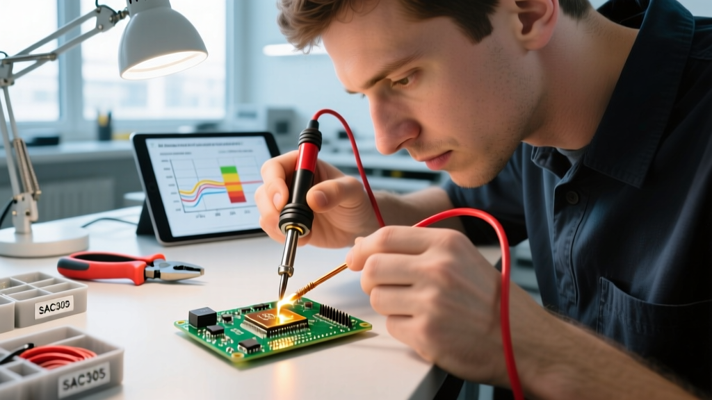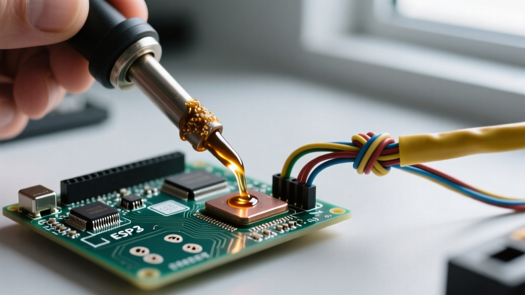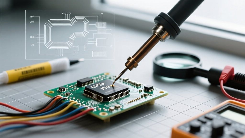

The Evolution of Industrial Soldering Joints in 2026
In the realm of consumer electronics, a functional connection is often sufficient. However, when designing for industrial applications—such as electric vehicle (EV) powertrains, aerospace avionics, and heavy machinery automation—the margin for error drops to absolute zero. Evaluating high-reliability soldering joints requires a deep understanding of metallurgy, thermal dynamics, and stringent compliance frameworks. As of 2026, the push toward higher operating temperatures and miniaturized power electronics has forced manufacturing engineers to rethink traditional surface mount technology (SMT) and through-hole methodologies.
Unlike standard commercial assemblies, industrial printed circuit board assemblies (PCBAs) must endure severe thermal cycling, high-frequency vibration, and corrosive environments. This guide dissects the anatomical requirements, alloy selections, and inspection protocols necessary to guarantee the longevity of critical soldering joints in high-stakes industries.
Defining Reliability: IPC Class 3 vs. NASA Standards
The baseline for industrial electronics is typically governed by the IPC-A-610 standard, specifically targeting Class 3 (High-Performance Electronic Products). Class 3 mandates that equipment must perform on demand, with no tolerance for downtime. However, for aerospace and defense applications, engineers frequently look to NASA-STD-8739.3, which dictates even more rigorous workmanship requirements for soldered electrical connections.
Critical Geometric Requirements
For a through-hole or surface mount soldering joint to meet Class 3 criteria, several geometric conditions must be met:
- Wetting Angle: The solder must exhibit a wetting angle of less than 90 degrees, indicating proper metallurgical bonding and flux activation.
- Fillet Concavity: The solder fillet must be concave, not convex. A convex fillet often masks a non-wetted condition or insufficient solder volume.
- Intermetallic Compound (IMC) Layer: While invisible to the naked eye, cross-section analysis must reveal an IMC layer (typically Cu6Sn5) between 1 to 3 microns thick. An IMC layer exceeding 4 microns becomes brittle and highly susceptible to mechanical shock.
"The integrity of a soldering joint is not determined by the volume of solder applied, but by the quality of the intermetallic bond formed during the liquidus phase. Excessive heat input grows the IMC layer, paradoxically weakening the joint it was meant to secure." — Advanced Materials in Electronics Manufacturing Journal
Metallurgy and Alloy Selection for Extreme Environments
Choosing the correct solder alloy is the first critical decision in industrial PCBA design. The transition to RoHS-compliant lead-free solders introduced significant challenges regarding thermal fatigue and tin whisker growth. Below is a comparison of the primary alloys utilized in high-reliability industrial applications today.
| Alloy Designation | Composition | Melting Point (°C) | Primary Industrial Application | Key Limitations |
|---|---|---|---|---|
| SAC305 | Sn96.5 / Ag3.0 / Cu0.5 | 217 - 220 | Standard industrial SMT, telecom, medical devices. | Prone to drop-shock fracture; requires higher reflow temps. |
| Sn63Pb37 | Sn63 / Pb37 (Eutectic) | 183 | Aerospace, defense, deep-well drilling (RoHS exempt). | RoHS non-compliant; lower tensile strength than SAC. |
| SAC405 | Sn95.5 / Ag4.0 / Cu0.5 | 217 - 221 | Automotive under-hood, high-vibration power electronics. | Higher cost due to silver content; increased wetting time. |
| Sn96.5Ag3.5 | Sn96.5 / Ag3.5 | 221 - 224 | High-temperature sensor arrays, industrial IoT. | Lack of copper can lead to pad dissolution on bare copper finishes. |
For automotive EV inverters, where operational temperatures can exceed 125°C, SAC305 is increasingly being replaced by SAC405 or specialized doped alloys (like SAC-Q) that include trace amounts of bismuth or nickel to inhibit IMC growth and improve thermal cycling resistance.
Thermal Profiling: Time Above Liquidus (TAL) and Peak Temperatures
Achieving the perfect soldering joint requires precise thermal profiling. Industrial boards often feature high thermal mass components, such as large copper pours, IGBT modules, and heavy aluminum heat sinks. These components act as heat sinks during the reflow process, leading to uneven heating and cold joints if not managed correctly.
Optimizing the Reflow Profile for SAC305
- Preheat Zone: Ramp rate should not exceed 2°C to 3°C per second to prevent solvent spattering and solder balling. Target 150°C.
- Soak Zone: Maintain 150°C to 190°C for 60 to 90 seconds. This allows the flux (typically a ROL0 or ROL1 no-clean formulation) to activate, remove oxides, and equalize the temperature delta between small SMDs and large BGA components.
- Reflow Zone (TAL): The Time Above Liquidus (217°C for SAC305) must be strictly controlled between 45 and 90 seconds. A TAL below 45 seconds results in incomplete wetting and grainy, disturbed joints. A TAL exceeding 120 seconds degrades the flux, causes excessive IMC growth, and risks delaminating the PCB substrate.
- Peak Temperature: Target 235°C to 245°C. Exceeding 250°C risks damaging the internal die of sensitive industrial microcontrollers.
Automated Inspection: Moving Beyond 2D Vision
In high-volume industrial manufacturing, manual inspection is obsolete and statistically unreliable. Modern facilities rely on a triad of automated inspection technologies to verify the integrity of soldering joints.
Inspection Technology Matrix
- 3D Solder Paste Inspection (SPI): Deployed immediately after stencil printing. Systems like the Koh Young KY8030-3 measure paste volume, area, and height using multi-frequency moiré phase-shift technology. Catching paste defects here prevents 70% of all end-of-line soldering defects.
- 3D Automated Optical Inspection (AOI): Post-reflow, 3D AOI systems inspect for visible defects: tombstoning, bridging, insufficient solder, and polarity errors. They utilize telecentric lenses and structured light to eliminate shadowing from tall industrial connectors.
- Automated X-Ray Inspection (AXI): Mandatory for Bottom Termination Components (BTCs) and Ball Grid Arrays (BGAs). While IPC-A-610 permits up to 25% voiding for standard BGA spheres, automotive and aerospace OEMs frequently mandate a strict <10% voiding threshold to ensure optimal thermal dissipation and mechanical shear strength.
Common Industrial Failure Modes and Mitigation Strategies
Even with optimized profiles, specific failure modes plague industrial soldering joints. Understanding these edge cases is vital for process engineers.
Head-in-Pillow (HiP) Defects
Common in BGA components, HiP occurs when the solder paste on the PCB pad and the solder sphere on the component melt but fail to coalesce, leaving a microscopic gap. This is often caused by component warpage during reflow or oxidized solder spheres. Mitigation: Utilize Type 4 or Type 5 solder paste with a highly active flux chemistry, and implement a nitrogen-enriched reflow oven (maintaining <1000 ppm O2) to prevent oxidation during the soak phase.
Thermal Fatigue and Cracking
Industrial equipment subjected to constant power cycling experiences coefficient of thermal expansion (CTE) mismatch between the silicon die, the FR-4 substrate, and the solder alloy. Over time, this induces shear stress, leading to micro-cracking in the soldering joints. Mitigation: Apply specialized underfill materials to BGAs and use conformal coating to stabilize surface mount components against vibrational shear.
Summary for Process Engineers
Engineering high-reliability soldering joints for industrial applications is an exercise in controlling variables. From selecting the appropriate silver-doped alloy and enforcing strict TAL limits, to deploying 3D AXI for subsurface void analysis, every step must align with IPC Class 3 or NASA workmanship standards. As power electronics continue to shrink and thermal densities rise, the mastery of these metallurgical and inspection principles will remain the defining factor between field success and catastrophic system failure.