
The High Stakes of Thermal Management in Industrial Soldering
In consumer electronics, a marginal solder joint might result in a returned gadget. In industrial applications—ranging from aerospace flight controllers to automotive EV inverters—a compromised joint can lead to catastrophic system failure, millions in liability, and severe safety hazards. Consequently, determining a good soldering temp is not merely a matter of melting solder; it is a precise metallurgical exercise governed by strict thermal profiling, alloy phase transitions, and rigorous industry standards.
For manufacturing engineers and high-reliability technicians in 2026, the definition of an optimal temperature window depends entirely on the solder alloy, the thermal mass of the printed circuit board (PCB), and the specific environmental stresses the final assembly will endure. This guide breaks down the exact temperature parameters required for industrial-grade soldering, moving beyond hobbyist guesswork into data-driven thermal management.
Defining a Good Soldering Temp by Alloy Composition
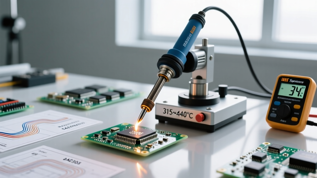
The most common mistake in industrial hand soldering and selective soldering is applying a universal temperature across different alloy chemistries. The liquidus and solidus points of your alloy dictate the baseline, but the actual iron or wave temperature must account for heat transfer efficiency and joint wetting dynamics.
| Alloy Designation | Composition | Melting Range (Liquidus) | Good Soldering Temp (Hand Iron) | Primary Industrial Application |
|---|---|---|---|---|
| SAC305 | Sn96.5 / Ag3.0 / Cu0.5 | 217°C - 220°C | 330°C - 360°C | General commercial/industrial (RoHS compliant) |
| Sn63/Pb37 | Tin / Lead (Eutectic) | 183°C | 300°C - 320°C | Aerospace, medical, military (Exempt from RoHS) |
| Sn95/Sb5 | Tin / Antimony | 232°C - 240°C | 350°C - 380°C | Under-hood automotive, high-temp industrial sensors |
| Sn10/Pb88/Ag2 | High-Lead / Silver | 268°C - 302°C | 380°C - 410°C | Die-attach, high-power RF amplifiers |
As outlined by the IPC Standards Directory, exceeding the recommended temperature by more than 30°C can cause rapid flux exhaustion and pad delamination, while under-shooting leads to incomplete wetting and high-resistance joints.
The Metallurgy of the Joint: IMC Layer Optimization
To truly understand what makes a good soldering temp, one must look at the microscopic level. Soldering is not just glue; it is a metallurgical bond. When molten solder contacts a copper pad, an Intermetallic Compound (IMC) layer forms—typically Cu6Sn5 initially, followed by Cu3Sn if heat is sustained.
Expert Insight: The ideal IMC layer thickness for a high-reliability industrial joint is between 1 and 3 micrometers. If your soldering temperature is too low or the dwell time is too short, the IMC layer remains incomplete, resulting in a weak, cold joint. If the temperature is too high or applied for too long, the IMC layer overgrows, becoming excessively thick and brittle, making the joint highly susceptible to mechanical shock and thermal cycling fractures.
According to guidelines published by the Surface Mount Technology Association (SMTA), maintaining the tip temperature strictly within the alloy's optimal window ensures the IMC layer grows at a controlled rate, maximizing both tensile strength and fatigue resistance.
Thermal Mass Challenges: Heavy Copper and Ground Planes
In industrial power electronics, such as motor drives and high-current distribution boards, PCBs frequently feature 2oz, 4oz, or even 6oz copper layers connected to massive internal ground planes. These act as enormous heat sinks, rapidly drawing thermal energy away from the soldering iron tip.
Protocol for High Thermal Mass Assemblies
- Preheating: Never apply a 400°C iron to a cold, heavy-copper board. The thermal shock can crack vias and delaminate the FR-4 substrate. Use a bottom-side preheater (e.g., Hakko FR-830) to bring the entire PCB ambient temperature up to 120°C - 130°C.
- Wattage over Temperature: A good soldering temp is useless without the thermal recovery rate to back it up. Use a high-wattage station (120W to 200W, such as the Weller WX2021 or JBC CD-2BQF) rather than simply turning up the dial on a 70W iron. Cranking a low-wattage iron to 400°C to compensate for thermal mass will oxidize the tip instantly and burn the flux before the joint reaches liquidus.
- Tip Geometry: Switch from fine conical tips to heavy chisel or bevel tips (e.g., Weller RTW032 or JBC C115-112) to maximize surface area contact and facilitate rapid heat transfer into the copper pour.
2026 Trends: Wide Bandgap Semiconductors and Extreme Temp Profiles
The rapid adoption of Silicon Carbide (SiC) and Gallium Nitride (GaN) power modules in EV and industrial solar applications has fundamentally shifted thermal requirements. These wide bandgap (WBG) semiconductors operate at junction temperatures exceeding 175°C, meaning standard SAC305 solder joints are at risk of creeping or melting under extreme transient loads.
For these cutting-edge 2026 assemblies, a good soldering temp often involves specialized high-temperature alloys like Sn95/Sb5 or even Transient Liquid Phase Sintering (TLPS) pastes. Hand soldering these modules requires precision profiling, often utilizing active-tip technology (like JBC's cartridge system) where the heater is integrated directly into the tip, ensuring zero thermal lag when touching massive SiC die-attach pads.
Failure Modes from Incorrect Temperature Profiling
Deviating from the optimal temperature profile introduces specific, identifiable failure modes. Inspecting these under an automated optical inspection (AOI) system or X-ray reveals the root cause:
- Cold Solder Joints (Too Low Temp / Insufficient Dwell): Characterized by a dull, grainy appearance and poor wetting angles (greater than 90 degrees). Electrically, these introduce micro-cracks that cause intermittent resistance spikes under vibration.
- Pad Lift and Measling (Too High Temp): Excessive heat degrades the epoxy resin in the PCB laminate, causing internal separation (measling) or completely lifting the copper pad from the substrate, destroying the board.
- Component Damage (Excessive Heat Transfer): Ceramic chip capacitors (MLCCs) are highly susceptible to thermal shock. Applying a 380°C iron directly to the terminal of a 1210 MLCC without preheating can induce micro-fractures in the dielectric, leading to latent short circuits months after deployment.
Compliance and Aerospace Workmanship Standards
In regulated industries, your temperature profile must be documented and repeatable. For aerospace and space-flight hardware, technicians must adhere to NASA Workmanship Standards (specifically NASA-STD-8739.3). These standards mandate that soldering irons be equipped with closed-loop temperature sensors and that operators verify tip temperatures with a calibrated thermocouple tester (such as the Hakko FG-100) at the start of every shift. A "good" temperature is only valid if it is verifiable and traceable.
Expert Troubleshooting Matrix
| Observed Symptom | Likely Thermal Cause | Corrective Action |
|---|---|---|
| Solder balls up and refuses to flow onto pad | Flux burned off due to excessive tip temp | Reduce iron temp by 20°C; apply fresh liquid or tacky flux |
| Joint looks grainy and dull (Leaded) | Movement during cooling or insufficient heat | Ensure fixture holds board still; increase tip size for better transfer |
| Tip oxidizes black within minutes | Idle temp too high or dry tip | Use standby/sleep mode (drop to 200°C when idle); always tin tip before holstering |
| IC pins short together (bridging) | Flux exhausted, temp slightly too low for drag soldering | Increase temp by 10°C; use a wider bevel tip and add no-clean flux gel |
Final Takeaways for Manufacturing Engineers
Achieving a good soldering temp in an industrial environment is a dynamic balancing act. It requires matching the iron's thermal recovery rate to the PCB's thermal mass, respecting the metallurgical limits of the chosen alloy, and strictly adhering to IPC and NASA workmanship standards. Invest in closed-loop, high-wattage soldering systems, mandate regular tip calibration, and never rely on visual guesswork when engineering high-reliability electronics.