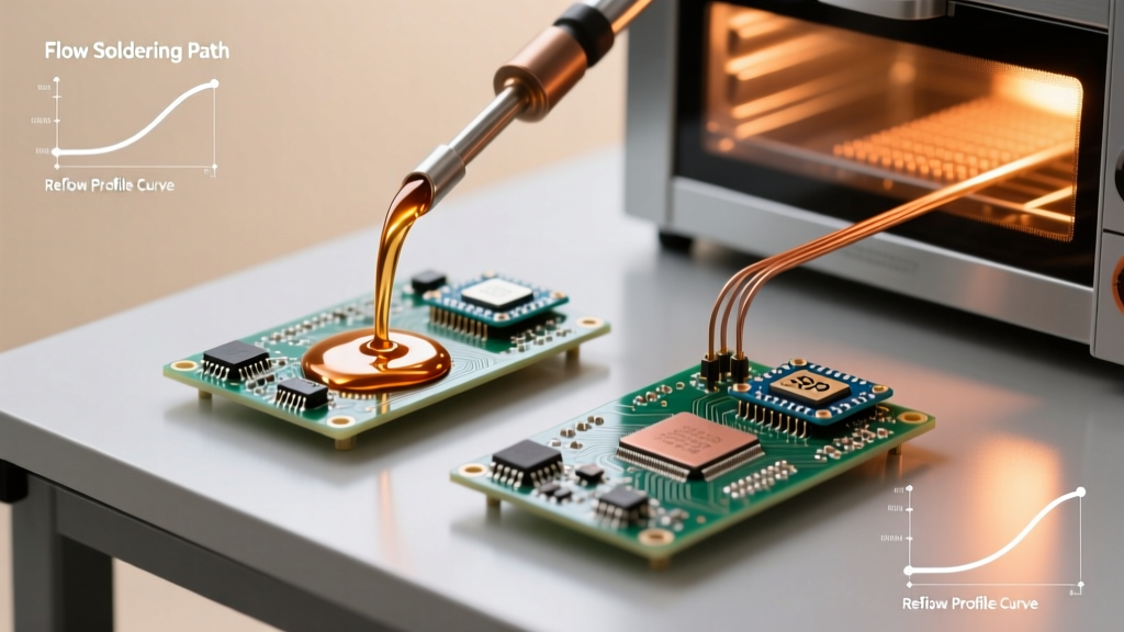

The Material Reality of Flow Soldering vs Reflow Soldering
When transitioning a printed circuit board (PCB) design from prototyping to volume manufacturing, the debate of flow soldering vs reflow soldering extends far beyond basic throughput metrics. At its core, this decision is governed by strict material compatibility. The thermal shock, dwell times, and chemical environments of flow (wave and selective) soldering differ radically from the controlled convection profiles of reflow ovens. Choosing the wrong process for your specific substrate, component packaging, or solder alloy can lead to catastrophic field failures, delamination, or catastrophic copper leaching.
This guide provides an in-depth material compatibility matrix and engineering framework to help PCB designers and manufacturing engineers align their board materials with the optimal soldering methodology.
Thermal Profiles: Convection vs. Direct Immersion
Understanding material compatibility requires analyzing how heat is transferred to the board. Reflow soldering relies on forced convection (and sometimes infrared or vapor phase) to gradually raise the entire PCB assembly to the alloy's liquidus temperature. A standard SAC305 (Tin/Silver/Copper) reflow profile features a controlled ramp rate of 1°C to 3°C per second, a soak zone to activate flux, and a peak temperature of roughly 245°C. The Time Above Liquidus (TAL) is tightly constrained to 45–90 seconds.
Conversely, flow soldering—encompassing both traditional wave soldering and modern selective flow nozzles—exposes the PCB to direct contact with molten solder. The solder bath typically operates between 260°C and 275°C. While the overall board temperature remains lower due to targeted application (especially in selective flow), the localized thermal shock at the point of contact is severe. This sudden delta-T is the primary enemy of brittle materials and multi-layer ceramic components.
PCB Substrate Compatibility Matrix
Not all laminates handle thermal stress equally. The Glass Transition Temperature (Tg) and Decomposition Temperature (Td) of your substrate dictate process viability. Below is a compatibility matrix for common 2026 PCB materials.
| Substrate Material | Typical Tg / Td | Reflow Compatibility | Flow / Wave Compatibility | Engineering Notes |
|---|---|---|---|---|
| Standard FR-4 | Tg 135°C / Td 310°C | Good | Poor (High Warpage Risk) | Prone to Z-axis expansion and pad cratering under wave thermal shock. |
| High-Tg FR-4 (e.g., Isola FR408HR) | Tg 180°C / Td 340°C | Excellent | Good | Industry standard for mixed-technology boards requiring selective flow. |
| Polyimide (Flex/Rigid-Flex) | Tg 250°C+ | Excellent (with fixtures) | Destructive | Direct molten flow will warp flex circuits unless heavy aluminum stiffeners and selective masking are used. |
| MCPCB (Aluminum Core) | N/A (Metal Core) | Poor (Requires specialized hotplates) | Excellent | Standard convection ovens cannot heat the massive aluminum heat sink. Flow/wave is the standard for LED lighting. |
| PTFE / Rogers (RF/Microwave) | High Thermal Stability | Good (Strict profiling needed) | Poor | Soft substrates can be physically eroded by the kinetic force of a turbulent solder wave. |
Component Package Constraints and the Shadowing Effect
Material compatibility also encompasses the physical geometry of the components soldered to the board. Reflow soldering is inherently compatible with ultra-fine-pitch Surface Mount Devices (SMDs). Packages like 0201 passives, Ball Grid Arrays (BGAs), and Quad Flat No-leads (QFNs) rely on the surface tension of molten paste to self-align during the reflow phase.
Flow soldering, however, introduces the shadowing effect. When a wave of solder hits a large component (like an electrolytic capacitor or a transformer), the turbulent flow is blocked, creating a "shadow" behind the component where solder fails to reach the pads. Furthermore, the kinetic force of a flow wave can easily shift unglued SMDs or cause micro-cracking in Multi-Layer Ceramic Capacitors (MLCCs) due to rapid thermal expansion mismatches.
Expert Insight: If your design requires both dense BGA/Fine-pitch SMDs and heavy Through-Hole Technology (THT) connectors, do not force the entire board through a flow wave. Utilize reflow for the SMD side, and employ selective flow soldering (using programmable mini-wave nozzles) strictly for the THT components to protect sensitive surface-mount materials.
Solder Alloy Selection: Dross, Leaching, and Wetting
The metallurgical compatibility of your chosen alloy shifts dramatically between the two processes. According to Indium Corporation's metallurgical data, the environment of a static reflow oven versus an agitated, oxygen-exposed flow bath changes alloy behavior.
Reflow Soldering Alloys
- SAC305 (Sn96.5/Ag3.0/Cu0.5): The undisputed king of reflow. The 3% silver content provides excellent drop-shock resistance and reliable wetting on OSP and ENIG finishes.
- Low-Temp BiSnAg (e.g., Sn42/Bi57.6/Ag0.4): Gaining massive traction in 2026 for sustainable manufacturing. Melts at ~138°C, drastically reducing energy consumption and protecting heat-sensitive substrates like PET flex circuits.
Flow Soldering Alloys
Using SAC305 in a high-volume wave or selective flow bath is a costly mistake. The high silver content accelerates copper leaching from the PCB pads (dissolving the copper traces into the bath) and generates expensive dross (oxidized slag) when agitated. Dross disposal and replenishment can cost manufacturing facilities upwards of $40 per pound.
- SN100C (Sn99.3/Cu0.7/Ni): The premier flow soldering alloy. The addition of Nickel stabilizes the bath, drastically reduces copper leaching, and minimizes dross formation. It is highly compatible with bare copper and HASL finishes.
- SAC0307 (Sn99.0/Ag0.3/Cu0.7): A low-silver alternative that balances joint reliability with bath economy, often used in selective flow applications.
Flux Chemistry and Residue Compatibility
Flux compatibility is often overlooked until post-solder cleaning failures occur. Reflow solder paste contains flux embedded within the solder powder (typically Type 3 or Type 4 mesh). The flux volume is precisely metered by the stencil aperture. No-clean rosin-based fluxes are standard, leaving a benign, non-conductive residue.
Flow soldering requires the application of liquid flux via spray or foam jets prior to the preheat zone. Because the board must pass through a turbulent wave, flow fluxes require higher solid content and more aggressive activators (often VOC-free water-based or alcohol-based resins) to prevent solder bridging. If a board features unsealed potentiometers, open-frame relays, or micro-switches, the aggressive capillary action of flow flux can wick toxic residues into the component internals, causing latent electrical failures. In such cases, reflow (or selective flow with precise drop-jet fluxing) is mandatory.
Real-World Failure Modes by Process
Adhering to IPC-A-610 and J-STD-001 standards requires recognizing process-specific failure modes tied to material incompatibility:
- Tombstoning (Reflow): Occurs when one pad of a small passive (like a 0402 resistor) heats faster than the other, causing the surface tension to pull the component upright. Caused by poor thermal mass balancing in the PCB layout, not the machine.
- Head-in-Pillow (Reflow): A BGA solder ball melts but fails to coalesce with the solder paste on the pad, usually due to oxidation or incompatible paste flux chemistry.
- Solder Icing / Bridging (Flow): Sharp, icicle-like formations on the board's trailing edge. This indicates incompatible preheat profiles (the flux solvents didn't fully evaporate, causing localized boiling when hitting the 265°C wave) or a degraded flux activator.
- Pad Cratering / Delamination (Both): While reflow causes Z-axis expansion delamination if the Tg is exceeded for too long, flow soldering causes localized pad cratering due to the sheer physical force of the wave hitting a brittle, high-Tg ceramic-filled laminate.
Summary Decision Framework
When finalizing your manufacturing strategy, use this rapid compatibility checklist:
- Choose Reflow if: Your board is >80% SMD, utilizes BGAs/QFNs, features flexible substrates, or relies on low-temperature BiSn alloys to protect heat-sensitive sensors.
- Choose Flow (Wave) if: You are manufacturing high-volume, single-sided legacy boards, aluminum-core LED panels, or simple through-hole power supplies where THT dominates.
- Choose Selective Flow if: You have a complex mixed-technology board (High-Tg FR-4) with dense SMDs on the top layer and heavy THT connectors on the bottom, requiring localized thermal application without a massive solder wave.
By aligning your substrate Tg, component geometry, and alloy metallurgy with the correct thermal delivery method, you eliminate the root causes of latent field failures and optimize your cost-per-board in high-volume production.