
Defining the Process: What Is Reflow Soldering?
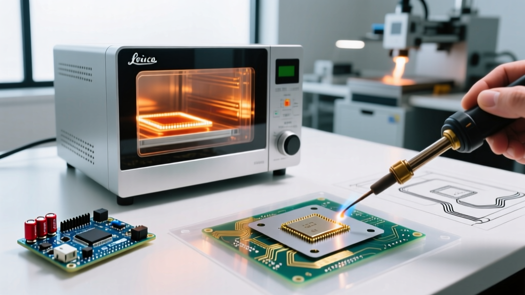
At its core, reflow soldering is the primary method used in modern Surface Mount Technology (SMT) to attach electronic components to printed circuit boards (PCBs). Unlike traditional methods that apply heat and solder simultaneously to a single joint, reflow soldering utilizes a pre-formulated solder paste—a viscous mixture of microscopic solder alloy spheres and chemical flux. This paste is applied to the board's pads, components are placed into the tacky paste, and the entire assembly is passed through a controlled thermal environment. The heat melts (reflows) the solder spheres, creating permanent metallurgical bonds as the board cools.
Understanding what is reflow soldering requires looking beyond the basic definition and examining the precise thermal chemistry involved. According to guidelines published by IPC standards, achieving a reliable intermetallic compound (IMC) layer between the component lead and the copper pad requires strict adherence to specific time-temperature profiles. For the industry-standard SAC305 (96.5% Tin, 3.0% Silver, 0.5% Copper) lead-free alloy, this means pushing the board past its 217°C melting point, typically peaking between 235°C and 245°C.
The 4-Stage Thermal Profile
A successful reflow process relies on a meticulously calibrated thermal profile, usually divided into four distinct zones inside the reflow oven:
- Preheat (Ramp-up): The board temperature is raised at a controlled rate of 1°C to 3°C per second to roughly 150°C. This prevents thermal shock to sensitive components like multilayer ceramic capacitors (MLCCs), which can crack under rapid temperature differentials.
- Thermal Soak: The board dwells between 150°C and 200°C for 60 to 120 seconds. This allows the entire assembly to reach thermal equilibrium and activates the flux, which cleans oxidation from the copper pads and component leads.
- Reflow (Peak): The temperature spikes past the solder's liquidus point (217°C for SAC305), peaking at 235°C–245°C for 30 to 60 seconds. The solder spheres collapse, wet the pads, and form the IMC layer.
- Cooling (Ramp-down): The board is cooled at a rate of 2°C to 4°C per second. Cooling too quickly induces thermal stress; cooling too slowly results in large, brittle grain structures in the solder joint.
Method Comparison Matrix: Reflow vs. Wave vs. Hand
To truly understand where reflow fits into the manufacturing ecosystem, we must compare it against the other dominant PCB assembly techniques. The table below outlines the critical operational differences.
| Parameter | Reflow Soldering (SMT) | Wave Soldering (THT) | Hand Soldering (Manual) |
|---|---|---|---|
| Primary Component Type | Surface Mount (SMD) | Through-Hole (THT) | Mixed / Rework / Prototyping |
| Setup Cost & Time | High (Stencils, Programming) | Medium (Fixtures, Pallets) | Low (Basic iron setup) |
| Per-Board Run Cost | Extremely Low at scale | Low at scale | Extremely High (Labor intensive) |
| Defect Rate (DPMO) | < 10 DPMO (Highly automated) | 50 - 200 DPMO (Bridging common) | Highly variable (Operator dependent) |
| Thermal Stress | Uniform (Whole board heated) | Localized but intense (Bottom heat) | Highly localized (Tip contact) |
Reflow Soldering vs. Wave Soldering
While reflow dominates SMT assembly, wave soldering remains relevant for through-hole components. In wave soldering, the populated PCB is passed over a standing wave of molten bulk solder (typically kept at 255°C to 265°C).
The primary disadvantage of wave soldering in modern, high-density designs is the 'shadowing effect.' If a tall component is placed in front of a shorter one, the wave cannot reach the pad of the shorter component, resulting in an open circuit. Furthermore, wave soldering cannot reliably process fine-pitch SMDs (like 0.4mm pitch QFNs or BGAs) without causing massive solder bridging. Reflow soldering entirely bypasses this issue because the solder is pre-deposited exactly where it is needed via a laser-cut stencil before the components are ever placed.
For mixed-technology boards containing both SMT and THT components, modern facilities use reflow for the SMT side, followed by selective soldering (a targeted, automated wave process) for the through-hole pins, completely avoiding the messy masking and palletizing required by traditional wave soldering.
Reflow Soldering vs. Hand Soldering
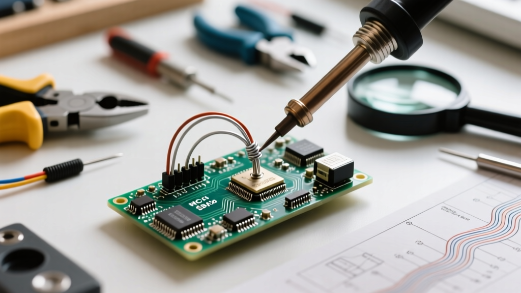
Hand soldering relies on a heated metal tip to transfer thermal energy directly to the joint, while simultaneously feeding a solid solder wire. It is indispensable for prototyping, rework, and low-volume bespoke assemblies. However, it lacks the repeatability of reflow.
When comparing the two, thermal mass management is the critical differentiator. In hand soldering, connecting a heavy ground plane to a small 0402 capacitor pad requires immense operator skill to prevent pad lift-off or component damage. Advanced soldering stations like the JBC CD-2BQE (approx. $650) or the Hakko FX-951 (approx. $250) utilize active tip sensing to inject heat rapidly, but they still rely on human judgment for wetting time and solder volume. Reflow soldering automates this: the solder paste volume is dictated by the stencil aperture and thickness (e.g., a 4-mil / 0.1mm thick stencil for 0402 components), and the heat is applied uniformly by forced convection in the oven.
Common Reflow Failure Modes and Edge Cases
Despite its high automation, reflow soldering introduces unique failure modes that do not exist in hand or wave soldering. Recognizing these is crucial for process engineers:
- Tombstoning (Drawbridge Effect): Common in small passives (0201, 0402). If one pad heats faster than the other, the flux on the hotter pad activates first, creating a surface tension imbalance that literally stands the component up on one end. Fix: Adjust the thermal soak time to ensure board-wide equilibrium, or reduce the stencil aperture on the pad connected to the heavy ground plane to reduce solder volume.
- Head-in-Pillow (HiP): A notorious BGA defect where the solder paste on the PCB pad melts, and the solder sphere on the BGA melts, but they fail to coalesce into a single mass, resting on top of each other like a head on a pillow. Fix: This is usually caused by insufficient peak temperature or oxidized BGA spheres. Utilizing a nitrogen-inerted reflow oven (maintaining < 500 ppm O2) drastically reduces oxidation and eliminates HiP.
- Solder Balling: Tiny spheres of solder splatter across the board. This occurs when the ramp-up rate during the preheat zone is too aggressive, causing the solvents in the flux to boil violently and eject microscopic solder particles. Fix: Flatten the initial ramp rate to 1°C/sec.
Capital Equipment and Consumable Costs
Transitioning to reflow soldering requires specific capital expenditure. For hobbyists or low-volume startups, benchtop reflow ovens like the T-962A can be acquired for roughly $250 to $300. While functional for basic boards, these lack the precise forced-convection airflow and multi-zone control of industrial units. Mid-tier batch ovens (e.g., LPKF ProtoFlow) range from $4,000 to $8,000, while high-volume inline conveyor ovens from manufacturers like Heller or BTU easily exceed $60,000 to $120,000.
Consumable costs are heavily tied to the materials. A custom laser-cut stainless steel stencil typically costs between $40 and $150 depending on the vendor and turnaround time. Solder paste is another recurring expense; a 500g jar of high-reliability SAC305 Type 4 paste from industry leaders like Indium Corporation or Alpha Assembly generally costs between $45 and $80. Because paste has a strict shelf life (usually 6 months refrigerated) and degrades once opened and exposed to ambient humidity, inventory management is a vital part of reflow economics.
Final Verdict on Method Selection
Ultimately, answering 'what is reflow soldering' reveals it as the undisputed champion of high-density, high-volume SMT manufacturing. While wave soldering retains a niche for heavy power through-hole components, and hand soldering remains the king of the prototyping bench and rework station, reflow provides the unmatched precision, speed, and joint reliability required for modern microelectronics. Selecting the right method depends entirely on your component mix, production volume, and capital constraints.