
The Metallurgy of Solderability: Why Solder Refuses to Wet
In electronics assembly and repair, a surface is considered solderable when molten solder can spontaneously spread and form a continuous intermetallic bond with the base metal. When you touch a 350°C iron tip to a pad and the solder beads up like water on a waxed car, you are witnessing a failure of wetting. According to the IPC standards body, true solderability requires a contact angle of less than 90 degrees, with high-reliability aerospace applications demanding angles under 45 degrees.
When a pad or component lead is non-solderable, the issue is rarely the solder alloy itself. Instead, it is almost always a metallurgical or chemical barrier preventing the flux from exposing bare metal to the molten tin, silver, and copper. Below, we break down the exact failure modes, diagnostic matrices, and step-by-step restoration protocols used by professional rework technicians in 2026.
The 5 Primary Culprits Behind Non-Solderable Surfaces
1. Severe Copper Oxidation (CuO vs. Cu2O)
Bare copper and Hot Air Solder Leveling (HASL) finishes oxidize over time. While mild cuprous oxide (Cu2O) is easily removed by standard rosin fluxes (ROL0 or ROL1), severe cupric oxide (CuO)—which appears as a dark, stubborn black or deep brown layer—requires aggressive organic acid (OA) fluxes or mechanical abrasion. Standard no-clean flux pens simply cannot penetrate heavy CuO layers.
2. ENIG 'Black Pad' Syndrome
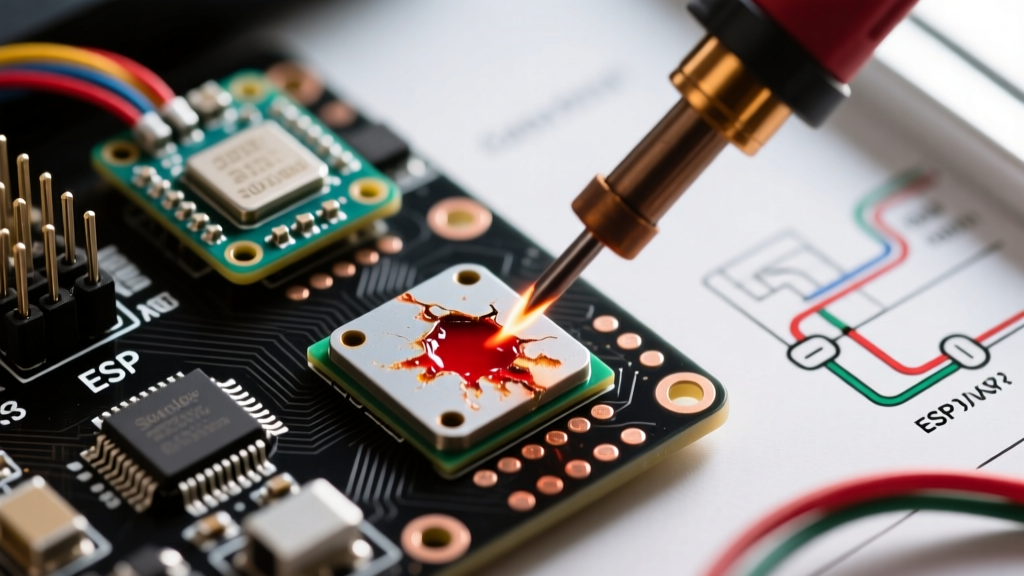
Electroless Nickel Immersion Gold (ENIG) is prized for its flat surface, but it is notorious for 'Black Pad' syndrome. This occurs when the gold immersion bath is too aggressive, causing hyper-corrosion of the underlying nickel layer. The pad looks perfectly golden, but when heated, the solder refuses to wet, or worse, it wets initially and then dewetts, leaving a brittle, phosphorus-rich nickel surface that guarantees field failure.
3. Silicone and Conformal Coating Residue
Even microscopic amounts of silicone off-gassing from nearby components, or residual acrylic/polyurethane conformal coating, will render a pad completely non-solderable. Silicone creates a thermally stable barrier that standard Kester or MG Chemicals fluxes cannot dissolve.
4. Intermetallic Compound (IMC) Exhaustion
If a pad has been reworked multiple times, the copper may have been entirely consumed, leaving only a thick, brittle layer of Cu6Sn5 intermetallic compound. Solder will not bond to an exhausted IMC layer; it will simply skate across the surface.
5. Matte Tin Oxidation on Component Leads
Modern lead-free ICs use matte tin finishes to prevent tin whiskers. However, matte tin oxidizes faster than bright tin. If an IC has been sitting in a non-climate-controlled warehouse for 18 months, the leads may appear dull gray and will reject solder unless pre-treated.
Troubleshooting Matrix: Symptoms and Corrective Actions
| Visual Symptom | Contact Angle | Probable Root Cause | Corrective Action |
|---|---|---|---|
| Solder forms perfect spheres | > 110° | Silicone contamination or heavy CuO | Solvent wash (IPA), then mechanical abrasion |
| Solder wets, then pulls back | 45° then >90° | ENIG Black Pad or flux burn-off | Strip finish, apply immersion tin or use high-activity flux |
| Solder sticks but looks dull/grainy | < 90° | Cold joint / IMC exhaustion | Scrape pad, add fresh SnPb or SAC305 solder to replenish alloy |
| Pad lifts during heating | N/A | Thermal delamination / Moisture | Pre-bake PCB at 105°C for 4 hours before rework |
Step-by-Step Restoration Protocol: Making Pads Solderable Again
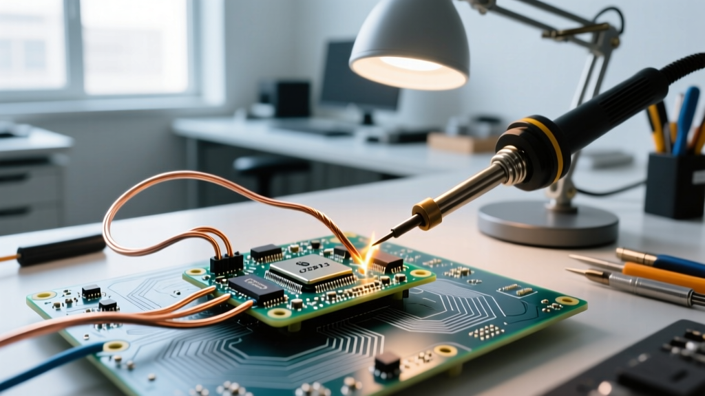
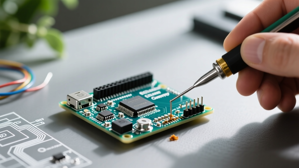
When you encounter a stubborn, non-solderable pad during a repair, do not simply turn up your soldering station to 450°C. Excessive heat will destroy the PCB's FR4 substrate and lift the pad. Follow this professional restoration workflow:
- Chemical Decontamination: Scrub the area with 99% Isopropyl Alcohol and a lint-free swab. If you suspect silicone, use a specialized cleaner like MG Chemicals 422C or a mild naphtha solvent.
- Mechanical Abrasion (If needed): For heavily oxidized HASL or bare copper, use a fiberglass scratch pen (such as the CircuitMedic Fiberglass Burnishing Pen, typically $14-$18). Gently brush the pad until the bright copper or underlying alloy is visible. Warning: Do not use fiberglass pens on ENIG or soft immersion silver, as you will strip the finish entirely.
- Flux Application: Apply a high-activity, mildly activated rosin flux. Kester 951 or Chip Quik NC191 (approx. $12 per pen) are industry standards for difficult wetting scenarios. Avoid 'no-clean' gels for initial wetting; liquid fluxes penetrate micro-fissures better.
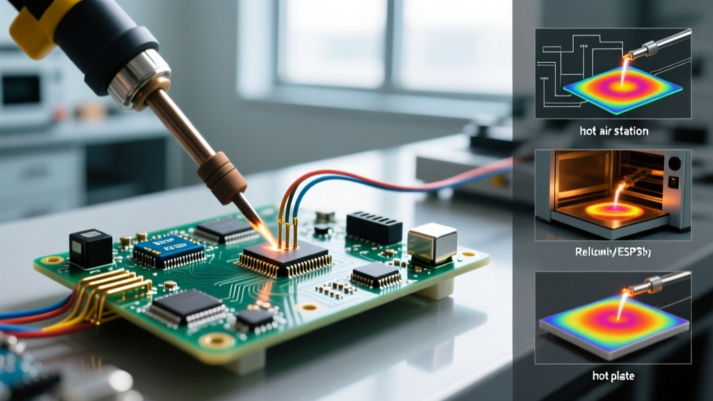
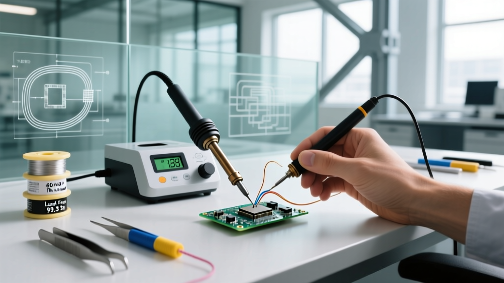
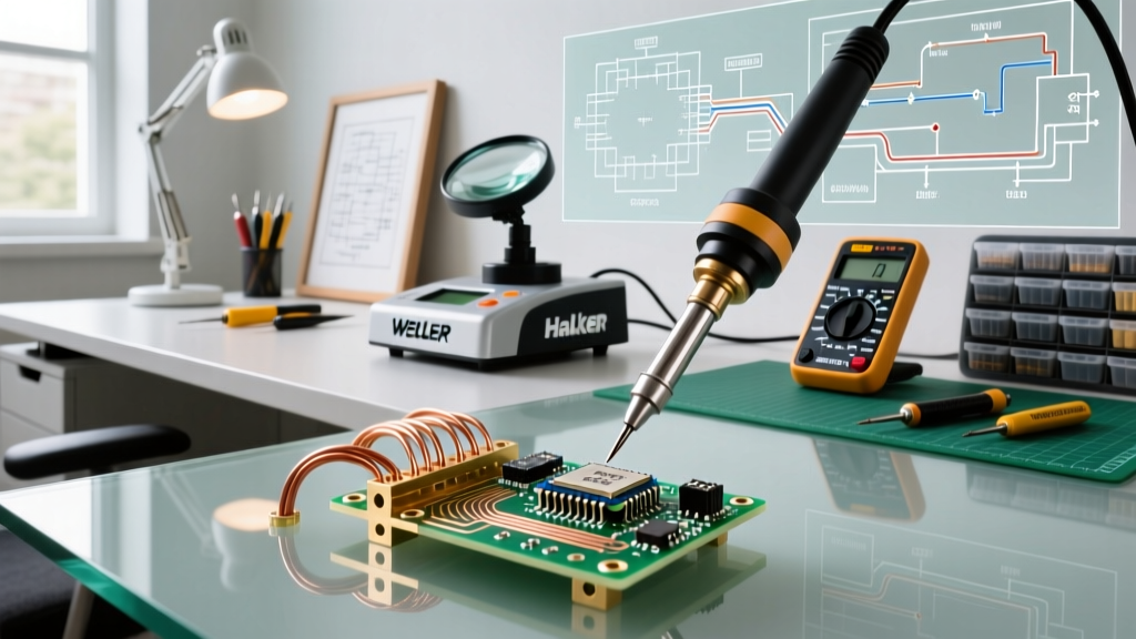
- Tinning the Pad: Set your station (e.g., Hakko FX-951 or JBC CD-2BE) to 320°C-340°C. Apply a small amount of fresh 63/37 SnPb solder (if leaded rework is permitted) or SAC305. The fresh solder acts as a bridge, dissolving the oxides and forming a new IMC layer.
- Cleanup: Once the pad is brightly tinned and wetted, clean the residual aggressive flux with IPA to prevent long-term dendritic growth or corrosion.
Expert Insight: According to guidelines published by the NASA Electronic Parts and Packaging (NEPP) program, attempting to solder to a non-wetting surface by adding excessive flux and heat is the leading cause of pad cratering and thermal damage to adjacent BGA components. Always restore the metallurgy first.
FAQ: Common Solderability Questions
How do I objectively test if a component lead is solderable before assembly?
For high-reliability or bulk manufacturing, technicians use the 'Dip and Look' test defined in IPC J-STD-002. The component leads are dipped in a specific flux, then immersed in a static solder pot maintained at 245°C ± 5°C (for SnPb) or 255°C (for SAC305) for exactly 5 seconds. Upon removal, the leads are inspected under 10x magnification. A continuous, smooth solder coverage of 95% or greater indicates the component is fully solderable. For DIYers, simply tinning a single corner lead with a well-fluxed iron is a sufficient proxy test.
Can flux make ANY metal solderable?
No. Flux is designed to remove oxides and prevent re-oxidation during heating; it does not alter base metallurgy. You cannot solder directly to aluminum, pure nickel, or titanium with standard electronics fluxes. These metals require specialized, highly corrosive acid fluxes (like zinc chloride) and specific alloy wires, and are generally not compatible with standard PCB assembly. Furthermore, as noted in CircuitNet's SMT troubleshooting archives, attempting to use plumbing acid flux on PCBs will result in catastrophic long-term galvanic corrosion.
What is the expected shelf life of solderability for different PCB finishes?
- ENIG (Electroless Nickel Immersion Gold): 12 to 15 months when stored in humidity-controlled environments (below 10% RH).
- HASL (Hot Air Solder Leveling): 6 to 12 months. The tin-lead or lead-free solder coating eventually oxidizes and interdiffuses with the copper.
- Immersion Silver: 6 to 9 months. Highly susceptible to sulfur-induced tarnishing if exposed to industrial air or cardboard packaging.
- OSP (Organic Solderability Preservative): 3 to 6 months. The organic layer degrades rapidly once exposed to UV light and ambient humidity.
Why does my solder wet the iron tip but ball up on the pad?
This is a classic thermal mismatch and oxidation issue. Your iron tip is tinned and hot, so the solder wets it. However, if the PCB pad acts as a massive heat sink (e.g., connected to a large ground plane) and your iron lacks the thermal recovery to bring the pad above the solder's liquidus temperature (183°C for SnPb, 217°C for SAC305), the flux will burn off before the pad is hot enough to form an intermetallic bond. Switch to a larger chisel tip to increase thermal mass transfer, or pre-heat the PCB to 100°C using a bottom-side preheater.