
The Anatomy of Bad Soldering Joints Across Assembly Methods
In the electronics manufacturing and DIY repair sectors, the phrase 'bad soldering joints' encompasses a wide spectrum of metallurgical and mechanical failures. Whether you are prototyping a custom PCB at your workbench or running a high-volume SMT (Surface Mount Technology) line, the fundamental requirement remains the same: achieving a proper intermetallic compound (IMC) layer between the copper pad and the component lead. According to the IPC Standards body, specifically the IPC-A-610 Rev H guidelines for electronic assemblies, a reliable joint must exhibit excellent wetting, a concave fillet, and a smooth, shiny appearance (for eutectic alloys) or a slightly dull, grainy texture (for lead-free alloys like SAC305).
However, the root causes of bad soldering joints vary drastically depending on the assembly method. Manual hand soldering relies on localized conductive heat transfer, while automated reflow and wave soldering depend on convective thermal profiling and fluid dynamics. Understanding these methodological differences is critical for accurate troubleshooting, defect reduction, and rework cost management.
Expert Callout: The IPC-A-610 Class 3 MandateFor aerospace, medical, and high-reliability automotive electronics, Class 3 standards dictate zero tolerance for certain bad soldering joints, such as disturbed joints or insufficient wetting. A wetting angle greater than 90 degrees is an immediate fail, indicating poor flux activation or inadequate thermal mass transfer.
Method 1: Hand Soldering (Manual Conductive Transfer)
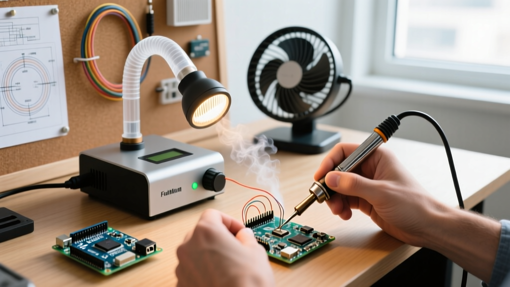
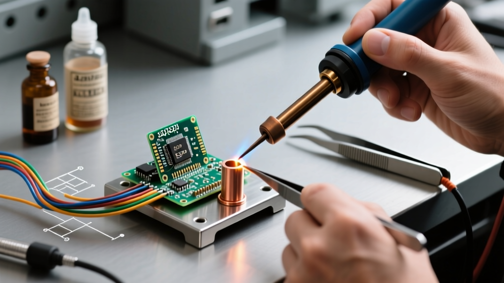
Hand soldering remains the backbone of prototyping, rework, and through-hole component assembly. The primary culprit behind bad soldering joints in this method is improper thermal management. Modern lead-free solders, such as SAC305 (Sn96.5/Ag3.0/Cu0.5), have a liquidus temperature of 217°C, requiring iron tip temperatures between 320°C and 350°C to ensure rapid wetting without burning the flux core.
Common Manual Failure Modes
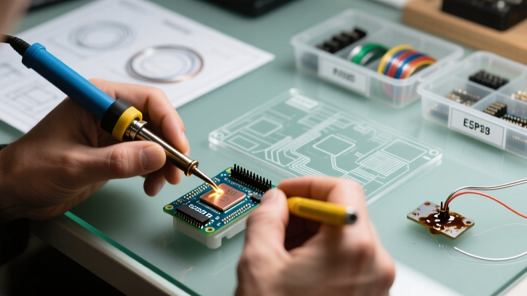
- Cold Joints: Characterized by a lumpy, convex, and dull appearance. This occurs when the iron tip temperature is too low, the tip is oxidized, or the joint is removed before the solder fully flows through the plated through-hole (PTH). The IMC layer fails to form properly, resulting in high electrical resistance and mechanical fragility.
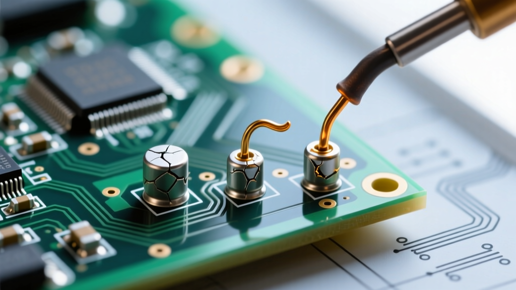
- Disturbed Joints: Often mistaken for cold joints, these exhibit a frosted or cracked appearance. They occur when the component or wire is moved while the solder is in the plastic (semi-solid) phase between liquidus and solidus temperatures. This fractures the crystalline structure of the cooling alloy.
- Solder Balls and Splatter: Caused by excessive moisture in the flux core or applying the solder wire directly to the iron tip rather than the joint. The rapid vaporization of flux volatiles explodes microscopic solder droplets onto adjacent pads, risking short circuits.
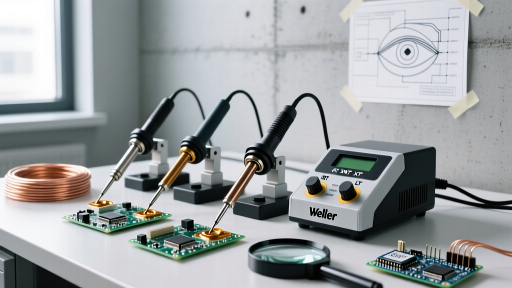
To mitigate these issues, technicians must match tip geometry to the thermal mass of the pad. For instance, using a micro-pencil tip (like the Weller RT4) on a large ground plane will result in a cold joint because the tip cannot replenish heat fast enough. A chisel or bevel tip is required to maximize surface contact area.
Method 2: Automated Reflow (SMT Convection Profiling)
Reflow soldering eliminates the human variable by baking the entire PCB assembly through a precisely calibrated thermal profile in a convection oven. Bad soldering joints in reflow are almost exclusively tied to profile deviations, paste stencil issues, or component warpage.
Reflow Profile Deviations and Defects
A standard lead-free reflow profile consists of four zones: Preheat, Thermal Soak, Reflow (Peak), and Cooling. The Time Above Liquidus (TAL) must be strictly maintained between 45 and 60 seconds.
- Tombstoning (Drawbridging): A classic SMT defect where a passive component (like a 0402 resistor) stands on one end. This happens when the solder paste on one pad melts before the other, creating uneven surface tension forces that pull the component upright. It is often caused by uneven pad geometry, incorrect stencil aperture reduction, or an aggressive ramp-up rate in the preheat zone.
- Head-in-Pillow (HiP): A notorious defect in BGA (Ball Grid Array) components. The solder paste melts and collapses, but the BGA solder ball does not fully coalesce with the paste due to PCB or component warpage during peak heating. Visually, the joint looks intact from the outside, but X-ray or cross-sectioning reveals a distinct boundary line—a catastrophic bad soldering joint that will fail under thermal cycling.
- Graping: When the solder paste fails to coalesce into a single smooth sphere, instead forming a cluster of oxidized micro-spheres. This is driven by flux exhaustion during an excessively long thermal soak phase, allowing the solder powder to oxidize before melting.
Method 3: Wave and Selective Soldering (THT Fluid Dynamics)
Wave soldering is utilized for high-volume through-hole components. The PCB passes over a standing wave of molten solder (typically at 260°C to 265°C for lead-free alloys). Here, bad soldering joints are driven by fluid dynamics, flux specific gravity, and shadowing effects.
Fluid Dynamic Failures
- Bridging and Webbing: Solder shorts between adjacent pins. This occurs when the solder pot temperature is too low (increasing viscosity), the conveyor speed is too fast, or the PCB lacks adequate 'thief pads' at the trailing edge of the wave to pull excess solder away from the IC leads.
- Icicles and Flags: Excessive solder that freezes into sharp spikes. This indicates poor flux activation, meaning the surface tension of the molten solder is too high to pull back cleanly into the pot. Checking the flux specific gravity and ensuring the preheat zone reaches 100°C-120°C to fully activate the rosin or organic acids is critical.
- Non-Filled PTH Barrels: The solder fails to wick to the top side of the board. According to NASA Workmanship Standards, Class 3 requires 100% barrel fill for high-reliability boards. Inadequate top-side preheating or oversized component leads in the barrel prevent capillary action from pulling the solder upward.
Comparative Matrix: Defect Origins and Detection
The table below contrasts how bad soldering joints manifest across the three primary methods and how modern 2026 inspection technologies catch them.
| Assembly Method | Primary Defect | Root Cause | 2026 Detection Method |
|---|---|---|---|
| Hand Soldering | Cold / Disturbed Joints | Insufficient tip thermal mass, operator movement | Visual Inspection, AI-Assisted Bench Cameras |
| Automated Reflow | Head-in-Pillow (HiP) | BGA warpage, TAL too short, paste volume low | 3D X-Ray Inspection (AXI) |
| Wave Soldering | Bridging / Icicles | Low pot temp, flux SG out of spec, no thief pads | Automated Optical Inspection (AOI) |
Rework Economics and the Cost of Bad Joints
The financial impact of a bad soldering joint scales exponentially depending on when it is detected. In 2026, the integration of AI-driven Automated Optical Inspection (AOI) systems on the production line has drastically reduced escape rates, but rework remains costly. The Surface Mount Technology Association (SMTA) frequently highlights the 'Rule of Ten' in defect economics:
- At the Paste Print Stage: Cost to correct is ~$0.10 (wipe and re-stencil).
- Post-Reflow (In-Line AOI): Cost to rework is ~$5.00 to $15.00 (requires hot-air rework station, flux, and skilled operator).
- Post-Wave (THT Rework): Cost is ~$10.00 to $25.00 (requires desoldering braid, PTH cleaning, and manual resoldering).
- In the Field (Warranty Return): Cost escalates to $500+ when factoring in shipping, diagnostics, system teardown, and brand reputation damage.
For DIY enthusiasts and small-batch repair shops utilizing hand soldering, the cost is measured in time and component destruction. Overheating a pad to fix a cold joint can easily lift the copper trace from the FR4 substrate, especially on cheaper, single-layer prototyping boards. Utilizing high-quality flux (such as Amtech NC-559-V2-TF) and properly tinning your iron tip with a sacrificial wire before applying heat to the target joint will reduce rework time by over 60%.
Final Troubleshooting Checklist
- Verify the Alloy: Are you using Sn63/Pb37 (183°C melt) or SAC305 (217°C melt)? Mixing them creates a bismuth-like low-melting eutectic phase that guarantees joint failure under thermal stress.
- Check the Oxidation: If the solder balls up and refuses to wet the pad, the pad is oxidized. Use a fiberglass scratch pen or isopropyl alcohol (IPA) and a brass brush to clean the copper before applying fresh flux.
- Monitor the Dwell Time: For hand soldering, a standard joint should take 2 to 3 seconds. If you are holding the iron for 7+ seconds, you are boiling the flux out of the paste or wire, guaranteeing a dry, oxidized, and mechanically weak connection.
Ultimately, whether you are managing a convection reflow profile or wielding a 65W Weller WE1010NA at your desk, eliminating bad soldering joints requires a strict adherence to thermal profiles, surface chemistry, and metallurgical best practices. Treat your flux as the actual hero of the process, and the solder as the structural result.