
The Art and Science of Soldering on Circuit Boards: An Expert Roundup
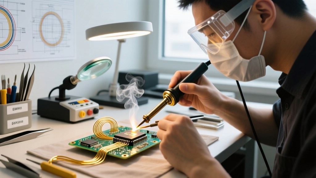
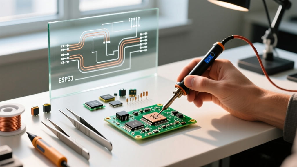
While automated Surface Mount Technology (SMT) lines handle the vast majority of commercial electronics manufacturing, manual soldering on circuit boards remains an irreplaceable skill. Whether you are prototyping a custom microcontroller board, executing high-reliability aerospace rework, or repairing a multi-layer motherboard, the physics of metallurgy and thermal transfer do not change. To bridge the gap between amateur hobbyist advice and professional manufacturing standards, we convened a virtual roundtable of three industry veterans to share their exact methodologies, tool preferences, and failure-analysis insights for 2026.
The Expert Panel
- Marcus Vance, IPC-A-610 Master Trainer: Specializes in high-reliability soldering standards, wetting angle analysis, and compliance for medical and aerospace PCB assemblies.
- Dr. Elena Rostova, PCB Failure Analysis Engineer: Focuses on the micro-structural integrity of solder joints, intermetallic compound (IMC) layer formation, and thermal shock diagnostics.
- Kenji Sato, Micro-Soldering Repair Specialist: Renowned for board-level component replacement, specializing in 0201 passives, BGA reballing, and high-density interconnect (HDI) trace repair.
Tooling: What Top Technicians Actually Buy
The era of relying on a generic 60W transformer-based iron is over. When soldering on circuit boards with mixed thermal masses, thermal recovery time is the single most critical metric. We asked our panel to evaluate the current market leaders based on real-world bench performance.
| Station Model | Price Range (2026) | Recovery Time | Tip Technology | Expert Verdict |
|---|---|---|---|---|
| JBC CD-2BQF | $550 - $620 | < 2 seconds | C245 Cartridge (Heater integrated) | "The undisputed king for heavy ground planes. The integrated heater eliminates thermal lag." - Vance |
| Hakko FX-951 | $260 - $310 | ~ 5 seconds | T18 (Sensor near tip) | "Reliable workhorse for general through-hole and standard SMD, but struggles with 4-layer boards." - Rostova |
| Pine64 Pinecil V2 | $26 - $30 | ~ 8 seconds | TS100 / 65W compatible | "Incredible for portable field repairs and hobbyists, but lacks the sustained thermal mass for continuous production." - Sato |
Metallurgy and Flux: The Chemistry of a Perfect Joint
According to Dr. Rostova, the most common mistake engineers make is treating flux as an afterthought. "Flux is not just a cleaning agent; it is a chemical catalyst that enables the metallurgical bond," she explains. When soldering on circuit boards, the goal is to form an Intermetallic Compound (IMC) layer between the copper pad and the solder alloy.
"An ideal IMC layer is between 1 and 3 microns thick. If your iron is too cool, the IMC doesn't form, resulting in a cold joint. If you dwell for more than 4 seconds, the IMC layer grows too thick, becoming brittle and prone to micro-fracturing under thermal cycling." — Dr. Elena Rostova
Expert Alloy and Flux Recommendations
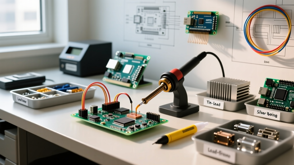
- Leaded Prototyping (Sn63/Pb37): Eutectic alloy melting at 183°C. It transitions instantly from liquid to solid, eliminating the "plastic" (mushy) phase where disturbed joints occur. Vance recommends Kester 245 mildly activated rosin flux for through-hole work.
- Lead-Free Production (SAC305): Melting point of 217°C. Requires higher iron temperatures (typically 350°C - 380°C) and highly active no-clean fluxes. Sato swears by Amtech NC-559-V2-TF for tacky SMD rework, noting its superior wetting properties on oxidized pads.
Thermal Management and Ground Plane Nightmares
One of the most frustrating edge cases when soldering on circuit boards is attempting to solder a component pin connected to a massive internal ground plane. The copper acts as a giant heatsink, pulling thermal energy away from the joint faster than the iron can supply it.
The "Thermal Relief" Myth and Preheating
Many CAD designers use thermal relief spokes on vias to aid manual soldering. However, in high-current or RF applications, solid copper pours are mandatory. "If you turn your iron up to 450°C to compensate for a ground plane, you will delaminate the FR-4 fiberglass and lift the pad before the solder flows," warns Vance.
The Expert Solution: Use a PCB preheater (such as the Hakko FR-830 or Puhui T-8280) to bring the entire board ambient temperature up to 120°C - 150°C. This reduces the thermal delta, allowing a 350°C iron to flow SAC305 solder in under 2.5 seconds without causing thermal shock to adjacent BGA chips or sensitive ceramics.
Micro-Soldering: Tackling 0201 and 01005 Passives
As consumer electronics shrink, manual rework on 0201 (0.6mm x 0.3mm) components has become a standard requirement. Kenji Sato outlines his precise workflow for these microscopic components:
- Optics: A trinocular stereo microscope with a 0.5x Barlow lens and ring LED illumination is non-negotiable.
- Tooling: Sato uses the JBC NT115 Nano handpiece with a 0.1mm conical tip (Tip 115-010). The ultra-low thermal mass prevents instantly vaporizing the flux.
- Flux Application: Never use a brush. Sato applies Amtech tacky flux using a 27-gauge precision syringe needle, placing a microscopic dot exactly between the pads.
- The Drag Technique: Tin only one pad. Use fine titanium tweezers to place the component. Touch the tinned pad for 0.5 seconds to anchor the part, release the tweezers, and then flow the second pad.
Expert Diagnostics: Identifying Failure Modes
When soldering on circuit boards goes wrong, the joint usually tells you exactly what happened. Our panel breaks down the visual diagnostics of common failures:
- Icicle / Solder Spike: Cause: Flux exhausted before the solder fully wetted, or iron temperature too low, causing high surface tension. Fix: Apply fresh liquid flux and reflow with a clean, tinned tip.
- De-wetting: Cause: Solder balls up and pulls away from the pad edge, leaving an irregular border. Usually caused by severe pad oxidation or contamination (finger oils). Fix: Clean with 99% IPA, apply aggressive RA (Rosin Activated) flux, and lightly scrub with a fiberglass scratch pen before re-tinning.
- Tombstoning (Drawbridging): Cause: Uneven heating during SMD soldering causes one side of the paste to reflow first, pulling the component upright via surface tension. Fix: Ensure symmetrical heat application or use a stencil with "home-plate" reduced-area pad designs to balance capillary forces.
- Pad Cratering: Cause: Mechanical stress combined with thermal shock. The copper trace separates from the underlying epoxy. Fix: Often fatal to the specific pad. Requires micro-drilling the via and running a 30AWG jumper wire to the next node.
Authoritative Resources and Standards
To deepen your understanding of professional soldering criteria, we highly recommend reviewing the foundational documents used by our expert panel. The IPC-A-610 Standard remains the global benchmark for the visual acceptability of electronic assemblies, detailing exact wetting angles and voiding limits. For those working with through-hole and basic wire terminations, the SparkFun Soldering Guide provides an excellent, highly visual baseline for hobbyists transitioning into professional prototyping workflows.
Frequently Asked Questions
What is the best temperature for soldering on circuit boards with SAC305?
While SAC305 melts at 217°C, your iron should be set between 350°C and 380°C. This provides enough thermal headroom to transfer heat rapidly into the joint within 2-3 seconds, minimizing the time the flux is exposed to high heat and preventing premature burnout.
How do I clean "no-clean" flux residue?
Despite the name, no-clean flux residues can become conductive or corrosive in high-humidity environments over time. Experts recommend cleaning it using a specialized saponifier or high-purity (99.9%) Isopropyl Alcohol combined with a lint-free swab, followed by a low-heat air dry to prevent the dissolved flux from wicking under BGA components.
Why does my solder look dull and grainy?
A dull, grainy appearance on lead-free solder is often normal due to the crystalline structure of SAC alloys cooling. However, if you are using eutectic Sn63/Pb37 (which should be shiny), a dull finish indicates a "disturbed joint"—meaning the component moved while the solder was in its plastic cooling phase, or the joint lacked sufficient heat to form a proper IMC layer.