
The Hidden Cost of Bad Soldering Examples in Modern Electronics
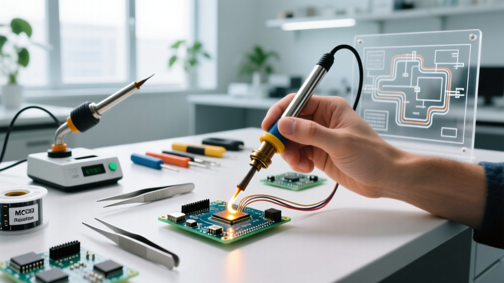
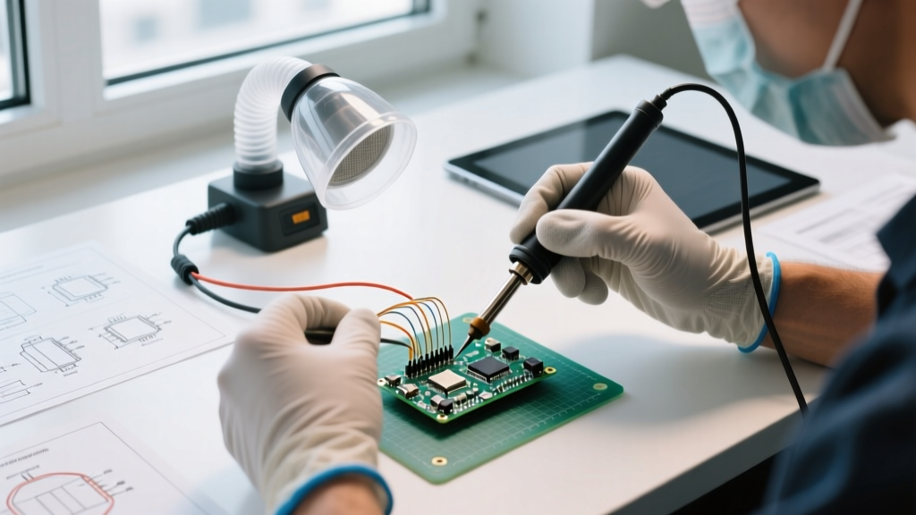
In the landscape of 2026 electronics manufacturing and DIY prototyping, the margin for error on printed circuit boards (PCBs) has never been smaller. With the industry standard shifting toward 0201 and 01005 surface-mount components and high-density interconnect (HDI) layouts, bad soldering examples are no longer just cosmetic blemishes—they are primary drivers of latent field failures, thermal runaway, and signal integrity loss. Whether you are building aerospace avionics or repairing a vintage audio amplifier, understanding the morphology of a failed solder joint is critical.
The gold standard for evaluating these defects is the IPC-A-610 (Acceptability of Electronic Assemblies) standard. This guide breaks down the physics of solder wetting, catalogs the 7 most common bad soldering examples, and provides actionable rework protocols using modern thermal tools.
The Physics of Wetting: What Makes a Joint 'Good'?
Before identifying defects, you must understand the metallurgical goal of soldering. A proper joint relies on wetting—the ability of molten solder to displace flux and form an Intermetallic Compound (IMC) layer with the copper pad and component lead. For standard SAC305 (lead-free) solder, this requires reaching a liquidus temperature of 217°C, though the iron tip is typically set to 340°C–360°C to account for thermal mass.
Expert Insight: The IMC layer (typically Cu6Sn5) should be microscopically thin. If the joint is too cold, the IMC fails to form (resulting in a cold joint). If the joint is overheated or the dwell time exceeds 4 seconds, the IMC layer grows too thick, becoming brittle and prone to mechanical fracturing under thermal cycling.
7 Bad Soldering Examples: Visual Defects and Rework Protocols
Below is a comprehensive diagnostic guide to the most frequent soldering defects encountered in both through-hole (PTH) and surface-mount (SMD) assemblies.
1. Cold Solder Joint (The High-Resistance Killer)
Visual Cue: The solder appears dull, gray, grainy, or lumpy. It fails to form a smooth concave fillet.
Root Cause: Insufficient heat transfer. This often happens when soldering a thick wire or a component connected to a large internal ground plane using an underpowered iron (e.g., a standard 40W ceramic heater). The solder melts from the iron's direct contact but the pad and lead never reach the activation temperature of the flux.
Rework Protocol: Do not simply add more solder. Apply a high-activity rosin flux (like Kester 951) to deoxidize the joint. Use a high-thermal-recovery station, such as a JBC CD-2BE with a C245 heavy chisel tip, set to 360°C. Heat the pad and lead simultaneously for 2-3 seconds until the existing solder flows like water, then remove the iron and hold the component perfectly still.
2. Solder Bridges (Accidental Shorts)
Visual Cue: A continuous blob of solder connecting two or more adjacent pads, creating a dead short.
Root Cause: Excessive solder application, using a tip that is too wide for the pitch (e.g., using a 2.4mm chisel on 0.5mm pitch SOIC pins), or dragging a dirty, oxidized tip across fine-pitch SMDs.
Rework Protocol: Apply No-Clean liquid flux to the bridged area. Take a high-quality copper desoldering wick (such as Goot Wick CP-2060, 2.0mm width) and press it gently over the bridge with a clean, tinned iron tip at 340°C. Capillary action will pull the excess solder into the braid. Clean the area with 99% isopropyl alcohol (IPA).
3. Disturbed Joints (Crystalline Fractures)
Visual Cue: A frosty, crystalline, or cracked appearance on the surface of the solder fillet.
Root Cause: Movement of the component or PCB during the critical phase transition from liquidus to solidus. Solder alloys are highly susceptible to micro-fracturing while cooling.
Rework Protocol: Secure the PCB in a heavy-duty vise or magnetic holder. Reflow the joint with fresh flux. For leaded Sn63/Pb37 solder, the plastic (semi-solid) phase lasts about 2 seconds; for SAC305, it can be slightly longer. Remove the heat and wait a full 5 seconds before releasing the board from the vise.
4. Insufficient Wetting (High Contact Angle)
Visual Cue: The solder balls up on the pad or lead with a contact angle greater than 90 degrees, resembling water on a waxed car hood.
Root Cause: Severe oxidation on the PCB pad or component lead, or the use of expired/weak flux that failed to strip the oxide layer before the solder melted.
Rework Protocol: Mechanically clean the pad with a fiberglass scratch pen if oxidation is severe. Apply a generous amount of tacky flux (e.g., Amtech NC-559-V2-TF). Reflow using a broad tip to maximize surface area heat transfer. As per SparkFun's soldering guidelines, proper pad preparation is 90% of the battle in achieving a low contact angle.
5. Excess Solder (The Hidden Pad Syndrome)
Visual Cue: A massive, convex blob of solder that completely obscures the component lead and the pad outline.
Root Cause: Overfeeding the solder wire. Beginners often mistake a large volume of solder for a 'strong' connection.
Rework Protocol: Under IPC-A-610 Class 3 (High-Performance) requirements, the contour of the lead must be visible through the solder fillet. Use an Edsyn Soldapullt DS017 desoldering pump to remove the bulk of the excess, then reflow the remaining solder with flux to achieve a proper concave shape.
6. Overheated Joints and Lifted Pads
Visual Cue: Scorched FR4 substrate, burnt black flux residue, or a copper pad that has partially peeled away from the fiberglass.
Root Cause: Dwell times exceeding 5 seconds, or using an iron set above 400°C on standard 1oz copper boards. The epoxy resin in the PCB degrades rapidly at high temperatures, destroying the bond to the copper.
Rework Protocol: If the pad is lifted but the trace is intact, carefully glue the pad down with two-part epoxy and use a 30 AWG copper wire to stitch the pad to the nearest via. To prevent this, utilize cartridge-based irons like the JBC tools ecosystem, which read the tip temperature 20 times per second, preventing the massive thermal overshoot common in older transformer-based stations.
7. Tombstoning (SMD Drawbridge Effect)
Visual Cue: A two-terminal SMD component (like a 0603 capacitor) stands straight up on one end, resembling a tombstone.
Root Cause: Uneven heating of the two pads. If one pad reaches reflow temperature before the other, the surface tension of the molten solder on the heated side pulls the component upright.
Rework Protocol: For manual rework, apply flux to both pads. Use a hot air rework station (like the Quick 861DW set to 380°C with a 3mm nozzle) to heat the entire component footprint evenly until the solder liquefies, then gently nudge the component flat with precision tweezers.
Defect Troubleshooting Matrix
Use this quick-reference table to diagnose and resolve issues on the workbench.
| Defect Type | Visual Indicator | IPC Class 3 Status | Primary Rework Tool |
|---|---|---|---|
| Cold Joint | Dull, grainy, lumpy | Reject | High-wattage cartridge iron (JBC/Hakko) |
| Solder Bridge | Shorted adjacent pads | Reject | 2.0mm Copper Desoldering Wick |
| Disturbed Joint | Frosty, cracked surface | Reject | PCB Vise + Flux + Reflow Iron |
| Insufficient Wetting | Contact angle > 90° | Reject | Fiberglass Pen + Tacky Flux |
| Excess Solder | Convex blob, hidden lead | Reject | Manual Desoldering Pump |
| Overheated / Lifted | Scorched board, lifted copper | Reject (Requires Repair) | Conductive Epoxy + 30 AWG Wire |
| Tombstoning | SMD standing vertically | Reject | Hot Air Station + Precision Tweezers |
Professional Rework Stations for 2026
Eliminating bad soldering examples requires moving beyond entry-level 45W irons. Modern rework demands active thermal feedback. Here are the top-tier stations dominating professional benches today:
- JBC CD-2BE (approx. $595): The undisputed king of SMD and micro-soldering. Its cartridge system houses the heating element inside the tip, offering zero-lag thermal recovery. Essential for 0201 components and dense BGA rework.
- Hakko FX-951 (approx. $285): A staple in mid-tier production and serious DIY labs. Uses T15/T18 tips and provides excellent, reliable performance for standard through-hole and mid-pitch SMD work.
- Quick 861DW (approx. $380): The best-in-class hot air rework station. Features programmable temperature curves and airflow settings, critical for preventing tombstoning and safely removing multi-pin QFP chips without scorching the FR4.
Conclusion
Recognizing and correcting bad soldering examples is what separates a hobbyist from a reliable electronics technician. By understanding the metallurgical requirements of the IMC layer, respecting the IPC-A-610 visual standards, and investing in thermal recovery tools, you can ensure every joint on your PCB is mechanically robust and electrically flawless. Always remember: flux is not optional, and patience during the cooling phase is mandatory.