
The Paradigm Shift: Why Socketed Memory Faded
If you built a PC in the late 1990s or early 2000s, upgrading your system memory was a trivial task. You simply unclipped the retaining arms of a DIMM slot, pulled out the old module, and pressed a new one into place. Today, however, the landscape of consumer and professional electronics has drastically changed. The prevalence of soldered on ram in everything from ultrabooks to Apple's M-series SoCs has fundamentally altered how we manufacture, use, and repair computing devices. But this transition was not born purely from a desire to limit consumer upgradability; it was driven by the unforgiving laws of physics and signal integrity.
As we navigate the hardware landscape of 2026, understanding the history of memory packaging is crucial for electronics technicians, PCB designers, and DIY repair enthusiasts. The journey from Dual In-line Package (DIP) chips to Socketed SIMMs/DIMMs, and finally to Ball Grid Array (BGA) soldering, represents one of the most significant shifts in modern motherboard design.
The Physics of High-Speed Memory and Signal Integrity
To understand why engineers moved toward soldered on ram, we must look at the evolution of memory speeds. Early DDR and DDR2 memory operated at relatively low frequencies (e.g., 400 MHz to 800 MHz). At these speeds, the electrical signals could easily travel from the CPU, through the motherboard traces, into a DIMM slot connector, and up the gold fingers of the RAM stick without significant degradation.
However, modern memory standards tell a different story. According to JEDEC's LPDDR5 and LPDDR5X specifications, data rates now exceed 8533 MT/s. At these multi-gigahertz frequencies, every millimeter of copper trace, every via, and every mechanical connector introduces parasitic capacitance and inductance. A traditional DIMM slot acts as a massive impedance discontinuity, causing signal reflections that corrupt data.
Engineering Reality Check: At DDR5 and LPDDR5X speeds, the trace length between the memory controller and the DRAM die must be minimized. By utilizing BGA soldering directly to the main PCB or an interposer, engineers eliminate the mechanical connector entirely, reducing trace lengths to mere millimeters and preserving signal integrity.
Manufacturing Soldered on RAM: SMT and BGA Profiling
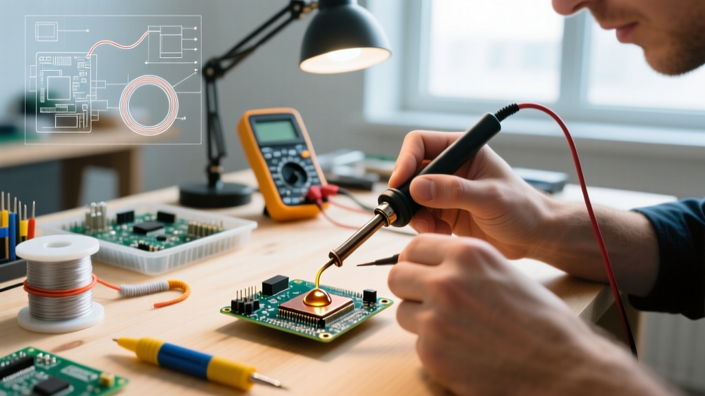
The transition to soldered on ram meant moving from through-hole and edge-connector mechanics to advanced Surface Mount Technology (SMT). Modern LPDDR chips are housed in BGA packages, where hundreds of microscopic solder spheres connect the chip to the PCB.
The SMT Assembly Process
In a high-volume manufacturing environment, soldering RAM to a motherboard involves a highly controlled process:
- Solder Paste Printing: A laser-cut stainless steel stencil is used to apply SAC305 (96.5% Tin, 3.0% Silver, 0.5% Copper) lead-free solder paste to the PCB pads.
- Pick-and-Place: High-speed SMT machines place the BGA memory chips onto the tacky flux with sub-millimeter precision.
- Reflow Soldering: The board passes through a multi-zone reflow oven. The thermal profile is strictly governed by IPC/JEDEC J-STD-020 standards, typically requiring a preheat zone (150°C), a soak zone to activate the flux, and a peak reflow temperature of 245°C to 250°C for a precise number of seconds.
- X-Ray Inspection: Because the solder joints are hidden beneath the chip, Automated Optical Inspection (AOI) is useless. Manufacturers use 3D X-ray systems to check for solder voiding and bridging. Under IPC-A-610 Class 2 standards, up to 25% voiding per solder ball is generally acceptable, but high-reliability computing often demands stricter internal thresholds.
Comparison Matrix: Memory Packaging in 2026
How does modern soldered memory compare to legacy socketed modules and the emerging CAMM2 standard? The table below breaks down the technical and practical differences.
| Feature | Socketed DDR5 DIMM | Soldered on RAM (BGA LPDDR5X) | CAMM2 (Compression Attached) |
|---|---|---|---|
| Max Practical Speed | ~6400 MT/s (Consumer) | 8533+ MT/s | ~7500 MT/s |
| Signal Integrity | Moderate (Connector impedance issues) | Excellent (Shortest trace lengths) | Very Good (Optimized compression) |
| Upgradability | High (End-user replaceable) | None (Factory fixed) | Moderate (Requires disassembly) |
| Rework Difficulty | Trivial (Slot replacement) | Extreme (Requires BGA rework station) | Low (Module replacement) |
| Typical Use Case | Desktop PCs, Workstations | Ultrabooks, Smartphones, Apple Silicon | Next-Gen Thin Gaming Laptops |
The Rework Reality: BGA Desoldering and Pad Cratering
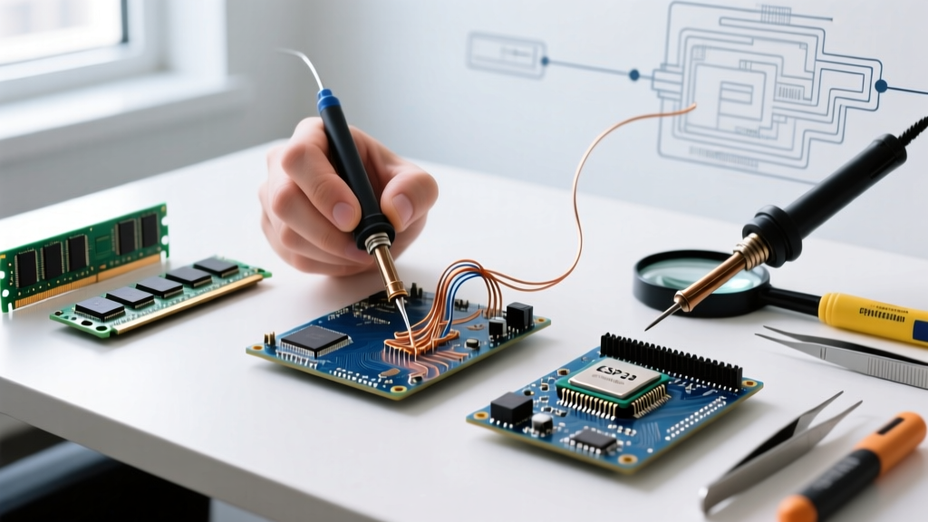
For the electronics repair community, the rise of soldered on ram has been highly controversial. As highlighted by the iFixit Right to Repair Manifesto, soldering critical components to the main board artificially limits the lifespan of a device if a single memory chip fails or if the user desires more capacity. However, with the right tools and expertise, BGA rework is possible, though fraught with risk.
Step-by-Step BGA RAM Replacement
Replacing a faulty soldered memory chip on a 2026 laptop motherboard requires professional-grade equipment, such as a Jovy Systems or Quick 863 BGA rework station. The process demands strict adherence to thermal profiles to avoid destroying the multi-layer PCB.
- PCB Preheating: The motherboard is clamped and preheated to 120°C - 130°C. This reduces the thermal gradient and prevents the board from warping when top heat is applied.
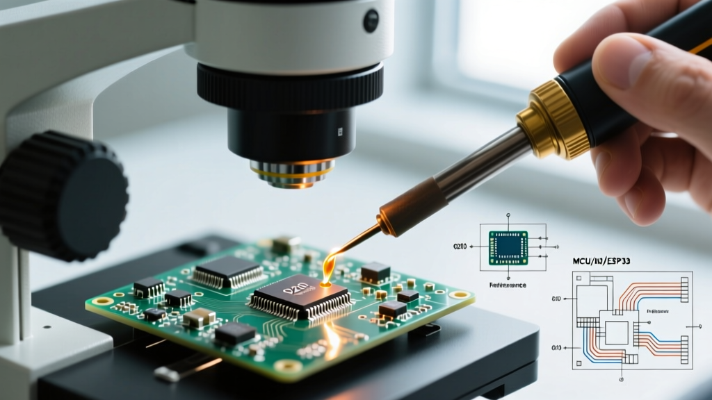
- Desoldering: Using a hot air nozzle profiled specifically for the BGA package size, the technician applies top heat (typically around 320°C - 350°C at the nozzle tip) while monitoring the board temperature. Once the solder melts (217°C for SAC305), the chip is lifted with a vacuum pickup tool.
- Pad Dressing: The remaining solder on the PCB is flattened using high-quality desoldering braid (e.g., Chemtronics or Goot Wick) and a temperature-controlled iron set to 350°C. Flux residue is cleaned with high-purity isopropyl alcohol.
- Reballing and Placement: The new or donor RAM chip is re-balled using a stencil and SAC305 solder spheres. Tack flux (like Amtech NC-559-V2-TF) is applied to the PCB, and the chip is aligned under a microscope.
- Final Reflow: The board undergoes a final reflow cycle, allowing the solder balls to collapse and form a reliable metallurgical bond.
Common Failure Modes in BGA Rework
Technicians attempting to replace soldered on ram must be wary of several catastrophic failure modes:
- Pad Cratering: Excessive mechanical force or rapid cooling can cause the copper pad to tear away from the underlying fiberglass laminate, destroying the PCB trace.
- Thermal Damage to Silicon: If the peak temperature exceeds 260°C for more than 10-15 seconds, the internal silicon die of the RAM chip can delaminate or suffer permanent thermal degradation.
- Solder Bridging: Misalignment during placement or excessive flux can cause adjacent microscopic solder balls to merge, resulting in a short circuit that prevents the system from posting.
The CAMM2 Standard: A Bridge Between Eras
By 2025 and 2026, the industry recognized the growing friction between the need for high-speed signal integrity and the consumer demand for repairability and upgradability. The solution championed by JEDEC is the CAMM2 (Compression Attached Memory Module) standard.
CAMM2 utilizes a specialized compression connector that sits incredibly close to the motherboard, mimicking the short trace lengths of soldered on ram while still allowing the user to unscrew and replace the memory module. While it does not completely replicate the ultra-thin Z-height of direct BGA soldering, it represents a vital compromise, offering LPDDR5X speeds without permanently fusing the memory to the logic board.
Conclusion
The evolution of soldered on ram is a testament to the relentless pursuit of performance in modern computing. As memory speeds push past the 8500 MT/s barrier, the mechanical DIMM slot has become a bottleneck that physics simply will not allow. While the shift to BGA soldering has undeniably complicated the repair landscape and challenged the Right to Repair movement, it has enabled the ultra-thin, high-performance, and power-efficient devices we rely on today. For electronics technicians and DIYers, mastering BGA rework and understanding high-speed signal integrity is no longer optional—it is a mandatory skill for navigating the future of hardware repair.