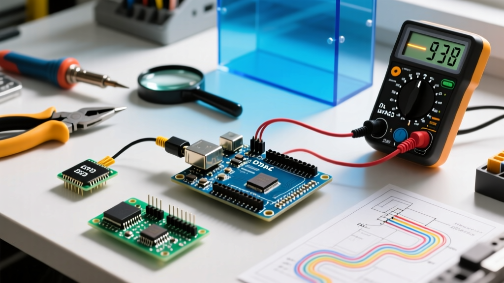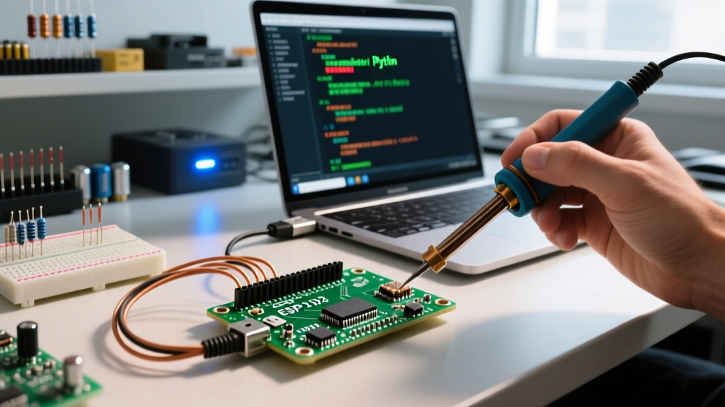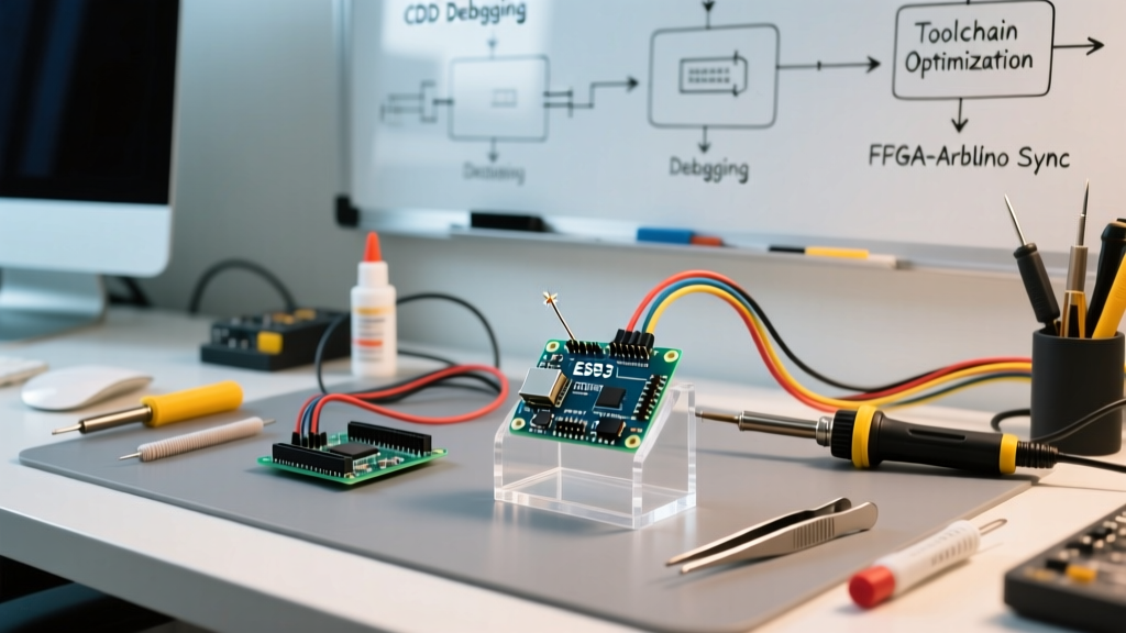

The Paradigm Shift: Sequential Control Meets Parallel Execution
Integrating an FPGA and Arduino architecture represents a massive leap in prototyping capabilities. While the Arduino ecosystem excels at sequential control, sensor polling, and rapid software iteration, Field Programmable Gate Arrays (FPGAs) offer deterministic, parallel hardware execution capable of processing high-speed data streams, custom DSP pipelines, and complex video manipulation. However, the primary bottleneck for most engineers is not the hardware itself, but the friction in the development workflow. Juggling disparate IDEs, mismatched voltage domains, and asynchronous clock boundaries can turn a weekend project into a month-long debugging nightmare.
This guide details a highly optimized, modern workflow for combining these two architectures, focusing on toolchain unification, interconnect protocols, and rigorous debugging methodologies to accelerate your hardware-in-the-loop (HIL) prototyping.
Hardware Selection: Purpose-Built vs. Modular Stacks
Your workflow efficiency begins with board selection. You generally have two paths: integrated development boards or modular stacks. Each dictates a different approach to power delivery, level shifting, and physical routing.
Option A: The Integrated Approach (Arduino MKR Vidor 4000)
The Arduino MKR Vidor 4000 remains a staple for unified workflows. It pairs a Microchip SAMD21 Cortex-M0+ microcontroller with an Intel Cyclone 10LP (10CL016) FPGA on a single PCB.
- Pros: Shared power rail, pre-routed high-speed internal buses, single footprint.
- Cons: The SAMD21 is aging (48MHz Cortex-M0+), and the Cyclone 10LP 16k logic elements (LEs) can feel restrictive for modern video processing. Retail price hovers around $110.
Option B: The Modern Modular Stack (Sipeed Tang Nano 9K + Arduino Nano ESP32)
For a more powerful, cost-effective 2026 workflow, pairing the Sipeed Tang Nano 9K (featuring the Gowin GW1NR-9C FPGA with 8,640 LUT4s and embedded PSRAM) with an Arduino Nano ESP32 is highly recommended.
- Pros: Massive processing headroom, dual-core 240MHz ESP32 for the MCU side, Wi-Fi/BLE connectivity, and a combined hardware cost of under $40.
- Cons: Requires manual level shifting and careful breadboard/PCB routing to maintain signal integrity at high frequencies.
Unifying the Toolchain for Speed
The traditional workflow of using the Arduino IDE alongside Intel Quartus or Xilinx Vivado is bloated and slow. To optimize your iteration cycles, transition to a unified, text-based toolchain driven by VS Code.
The Optimized Software Stack
- MCU Firmware: Use PlatformIO within VS Code. It provides autocompletion, CMake integration, and rapid OTA (Over-The-Air) flashing capabilities via the ESP32.
- FPGA RTL & Synthesis: Adopt the OSS CAD Suite. This open-source suite includes Yosys (synthesis), nextpnr (place and route), and Verilator (simulation).
- Simulation: Ditch heavy commercial simulators for quick logic checks. Verilator compiles Verilog/SystemVerilog into highly optimized C++ models, allowing you to co-simulate your Arduino C++ logic and FPGA RTL in a single desktop environment before ever touching the hardware.
Workflow Rule of Thumb: Never flash an FPGA to test basic state-machine logic. If it takes more than 30 seconds to synthesize and route, you are wasting time. Write a Verilator testbench to validate the RTL in milliseconds.
Overcoming the Interconnect Bottleneck
When bridging an FPGA and Arduino, the communication protocol dictates your system's maximum throughput. Selecting the wrong protocol is the most common workflow killer, leading to dropped packets and buffer overruns.
| Protocol | Max Theoretical Speed | Real-World Throughput | Pin Count | Best Use Case |
|---|---|---|---|---|
| UART | 1 Mbps | ~80 KB/s | 2 (TX/RX) | Telemetry, low-speed config commands |
| I2C | 1 MHz (Fast Mode) | ~100 KB/s | 2 (SDA/SCL) | Register configuration, sensor polling |
| SPI | 20+ MHz | 1.5 - 2.5 MB/s | 4 (MOSI/MISO/SCK/CS) | Bulk data transfer, audio streams, DMA |
| 8-Bit Parallel (FSMC) | 50+ MHz | 10+ MB/s | 12+ (Data + Ctrl) | High-res video, ADC data arrays |
For most sensor-fusion and DSP applications, SPI is the optimal middle ground. As detailed in SparkFun's SPI protocol guide, SPI allows full-duplex communication. To optimize the workflow, configure the Arduino ESP32 to use hardware DMA (Direct Memory Access) for SPI transfers. This frees the MCU's CPU to handle network stacks while the FPGA streams data directly into the ESP32's RAM buffers.
Critical Edge Cases: CDC and Voltage Translation
Rapid prototyping often leads to sloppy hardware integration, resulting in silent failures that consume days of debugging. Address these two edge cases immediately in your design phase.
1. Voltage Domain Mismatches
The Arduino Nano ESP32 operates at 3.3V, while many legacy sensors and generic FPGAs might utilize 1.8V or 5V IO banks. Directly connecting a 5V Arduino Uno R3 to a 1.2V/3.3V FPGA IO bank will destroy the FPGA's input clamping diodes.
- Optimized Solution: Use bidirectional level shifters like the TXB0106 (for low-speed GPIO/I2C) or the SN74AVC4T245 (for high-speed SPI/Parallel buses). The SN74AVC series supports data rates up to 200 Mbps, ensuring your logic translator does not become the bottleneck in your SPI bus.
2. Clock Domain Crossing (CDC)
The FPGA operates on a high-frequency, low-jitter crystal oscillator (e.g., 27MHz or 48MHz), while the Arduino's SPI clock is asynchronous and phase-drifting. Passing an SPI data line directly into the FPGA's 100MHz internal logic without synchronization causes metastability, leading to erratic state-machine behavior.
- Optimized Solution: Always implement a 2-Flip-Flop (2-FF) synchronizer for all asynchronous control signals entering the FPGA fabric. For multi-bit data buses (like SPI payloads), use asynchronous FIFOs (First-In-First-Out buffers) with Gray-code pointers to safely cross the clock boundary.
The Optimized 4-Step Deployment Pipeline
To maintain momentum during complex builds, adopt this strict four-step pipeline to isolate faults quickly.
- RTL Co-Simulation (Day 1): Write the FPGA Verilog and a C++ testbench using Verilator. Mock the Arduino's SPI inputs in C++ and verify the FPGA's DSP output. Goal: 100% logic validation before hardware.
- FPGA Loopback Test (Day 2): Flash the FPGA. Write a simple Arduino sketch that sends an incrementing byte pattern via SPI. The FPGA immediately echoes it back. Use a Saleae Logic Pro 8 to physically probe the SPI lines and verify timing margins and voltage levels. Goal: Validate the physical interconnect.
- Hardware-in-the-Loop Integration (Day 3): Integrate the actual sensor or DSP payload. Utilize the FPGA's built-in Integrated Logic Analyzer (ILA) or Gowin's GAO (Gowin Analyzer Oscilloscope) to capture internal FPGA signals in real-time and export them as VCD (Value Change Dump) files for GTKWave analysis. Goal: Debug internal timing violations.
- System-Level Stress Testing (Day 4): Run the full system for 24 hours. Monitor the ESP32's free heap memory to ensure DMA buffers aren't leaking, and check the FPGA for thermal throttling if utilizing high-density logic blocks.
Conclusion
Combining an FPGA and Arduino architecture unlocks unparalleled prototyping power, bridging the gap between software flexibility and hardware determinism. By abandoning legacy IDEs in favor of PlatformIO and OSS CAD Suite, carefully selecting high-throughput SPI interconnects, and rigorously managing clock domain crossings, you eliminate the friction that traditionally stalls hybrid MCU-FPGA projects. Implement this workflow to transform your next embedded systems project from a frustrating debugging exercise into a streamlined, predictable engineering success.