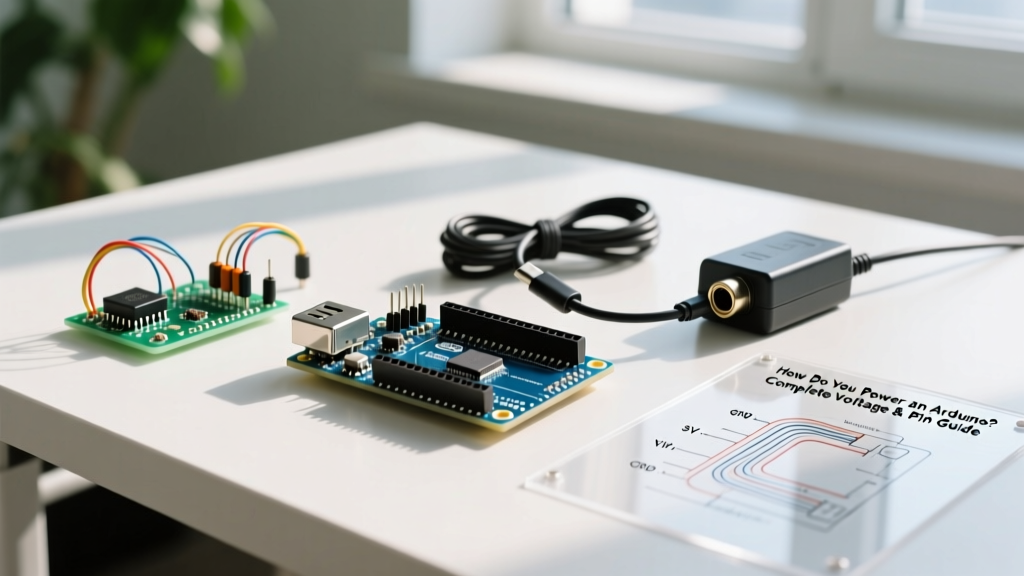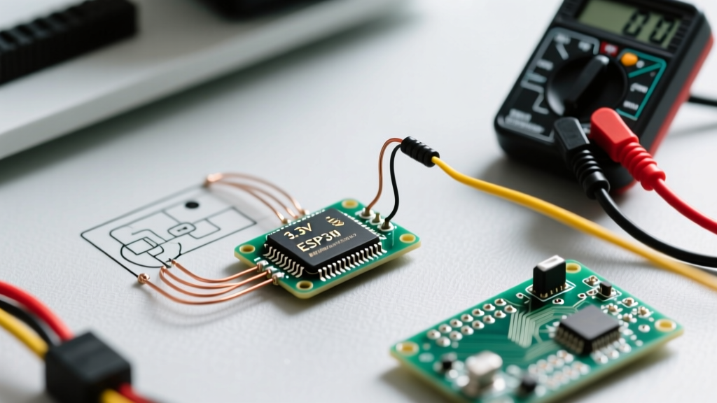

The Paradigm Shift: 5V AVR to 3.3V ARM Architectures
For over a decade, the 5V ATmega328P-based Arduino Uno R3 was the undisputed baseline for maker electronics. In that 5V ecosystem, configuring an arduino pull up resistor was straightforward: a standard 10kΩ or 4.7kΩ through-hole resistor reliably held logic lines high, and the microcontroller's robust 5V tolerant GPIO pins handled the rest. However, as we navigate the hardware landscape of 2026, the industry standard has decisively shifted toward 3.3V ARM Cortex-M and RISC-V architectures. Boards like the Arduino Nano RP2040 Connect, the Nano 33 BLE Sense (nRF52840), and various ESP32-S3 variants now dominate prototyping and commercial IoT deployments.
Migrating your legacy 5V designs to these modern 3.3V platforms is not a simple drop-in replacement. The physics of logic thresholds, bus capacitance, and current sinking change dramatically when VCC drops from 5.0V to 3.3V. If you attempt to port a legacy shield or wiring harness without recalculating your pull-up strategy, you will inevitably encounter floating inputs, I2C NACK errors, and ghosting in switch matrices. This guide provides a rigorous, engineering-focused framework for upgrading your pull-up networks for the 3.3V era.
Internal vs. External: Evaluating the Arduino Pull Up Resistor
The Arduino IDE abstracts hardware configuration through the pinMode(pin, INPUT_PULLUP) function. While convenient, relying on internal silicon resistors for critical timing or noisy environments is a common migration pitfall. Internal pull-ups are manufactured with wide tolerance bands and vary significantly between silicon families.
Silicon Comparison: Internal Pull-Up Specifications
When migrating from an older AVR board to a modern ARM or Xtensa-based MCU, you must account for the differing internal resistance values. Below is a comparison of the internal pull-up characteristics across popular architectures used in the Arduino ecosystem.
| MCU Architecture | Common Board Example | Internal Pull-Up Range | Software Pull-Down Support | Max GPIO Sink Current |
|---|---|---|---|---|
| ATmega328P (8-bit AVR) | Arduino Uno R3 | 20kΩ - 50kΩ | No (Hardware only) | ~10mA per pin |
| RP2040 (Dual ARM M0+) | Nano RP2040 Connect | 50kΩ - 80kΩ | Yes (Native) | ~4mA per pin |
| nRF52840 (ARM M4F) | Nano 33 BLE Sense | 11kΩ - 16kΩ | Yes (Native) | ~5mA per pin |
| ESP32-S3 (Xtensa LX7) | ESP32-S3 DevKitC | 35kΩ - 55kΩ | Yes (Native, limited pins) | ~6mA per pin |
Source: Refer to the official RP2040 Datasheet and Arduino Digital Pins Documentation for exact silicon tolerances and pin multiplexing limitations.
Migration Insight: Notice that modern 3.3V ARM chips natively support software-configurable pull-down resistors, a feature entirely absent in the legacy ATmega328P. This allows you to invert your switch logic in firmware without rewiring the physical PCB, provided your external circuit does not hard-wire a 5V pull-up that would back-feed and destroy the 3.3V GPIO.
Recalculating External I2C Pull-Up Values for 3.3V Logic
The most critical failure point during a 5V to 3.3V migration is the I2C bus. I2C is an open-drain protocol; it relies entirely on external pull-up resistors to return the SDA and SCL lines to a logical HIGH. According to the NXP I2C Specification (UM10204), the rise time of the bus is dictated by the RC time constant formed by the pull-up resistor and the total bus capacitance (trace capacitance + pin capacitance of all devices).
The Math Behind the Migration
In a 5V system, a 4.7kΩ resistor was the default choice. It provided a safe sink current of roughly 1mA (5V / 4.7kΩ), well within the ATmega328P's limits, while charging a typical 100pF bus capacitance fast enough for 100kHz Standard Mode.
When you drop VCC to 3.3V, that same 4.7kΩ resistor only supplies 0.7mA of charging current. If your bus capacitance exceeds 50pF, the RC rise time will stretch beyond the 1000ns maximum allowed for Standard Mode, resulting in corrupted bytes and NACK errors. You must lower the resistance to increase the charging current, but you cannot exceed the MCU's maximum sink current (typically 3mA to 6mA for modern 3.3V ARM chips).
- Minimum Resistance Calculation (3.3V, 3mA max sink): R = V / I → 3.3V / 0.003A = 1,100Ω.
- Optimal 100kHz (Standard Mode) Value: 3.3kΩ (Provides 1mA sink, excellent noise immunity).
- Optimal 400kHz (Fast Mode) Value: 2.2kΩ (Provides 1.5mA sink, faster rise times for higher capacitance).
Actionable Upgrade: Desolder all legacy 4.7kΩ axial resistors from your I2C lines. Replace them with 2.2kΩ or 3.3kΩ resistors. For permanent shield migrations in 2026, abandon through-hole components in favor of SMD resistor networks like the Bourns 4608X-101-332LF (an 8-pin SIP network containing eight 3.3kΩ resistors). At approximately $0.15 per unit in low volumes, they save massive amounts of board real estate and reduce parasitic inductance compared to axial leads.
Button Matrices and Ghosting: Edge Cases in 3.3V
Keypad matrices (e.g., 4x4 membrane switches) rely on a combination of driven rows and pulled-up columns. In legacy 5V designs, the high voltage threshold (V_IH) of the ATmega328P was roughly 3.0V (0.6 x VCC). This provided a massive 2.0V noise margin against electromagnetic interference (EMI) from nearby relays or motors.
On a 3.3V RP2040 or nRF52840, the V_IH threshold drops to approximately 2.0V to 2.3V. Your noise margin is suddenly cut in half. If your matrix wiring runs parallel to unshielded PWM motor lines, the reduced noise margin will cause 'ghosting'—phantom button presses registered by the MCU.
Hardware Mitigation Strategies
- Decrease Pull-Up Resistance: Drop from the internal ~50kΩ to an external 10kΩ discrete array. This stiffens the logic line, making it harder for capacitive crosstalk to induce a voltage spike that crosses the 2.0V V_IH threshold.
- Implement Software Debouncing Hysteresis: Do not rely solely on hardware. Implement a moving-average digital filter or a strict state-machine debounce routine requiring 3 consecutive identical reads spaced 5ms apart before registering a state change.
- Use I2C GPIO Expanders: For complex matrices, offload the scanning to an I2C expander like the NXP PCA9548A or Microchip MCP23017. These chips feature dedicated, highly regulated internal pull-ups and Schmitt-trigger inputs that restore the noise margins lost in the 3.3V migration.
Common Migration Failure Modes and Troubleshooting
When upgrading your workbench from 5V to 3.3V, keep this troubleshooting matrix handy to diagnose pull-up related anomalies.
| Symptom | Probable Cause in 3.3V Migration | Engineering Solution |
|---|---|---|
| I2C devices randomly drop off bus or return 0xFF | Rise time too slow due to 4.7kΩ pull-ups on high-capacitance 3.3V bus. | Reduce pull-up to 2.2kΩ. Verify bus capacitance is under 400pF. |
| GPIO reads erratic HIGH when button is open | Internal pull-up (50kΩ+) too weak for noisy 3.3V environment. | Add external 10kΩ discrete pull-up resistor to 3.3V rail. |
| MCU Brownout / Reset when button pressed | Pull-up resistor value too low (e.g., 100Ω), drawing >30mA when shorted to ground. | Recalculate using Ohm's law. Never use less than 1kΩ for direct GPIO pull-ups. |
| Back-feeding 5V into 3.3V MCU | Legacy shield uses hardwired 5V pull-ups on shared data lines. | Cut 5V pull-up traces on shield. Install level-shifter (e.g., TXS0108E) or rewire to 3.3V. |
Summary: Best Practices for 2026 Prototyping
Migrating your arduino pull up resistor strategy from 5V to 3.3V is a fundamental requirement for modern embedded design. The days of blindly tossing a 10kΩ resistor onto a breadboard and expecting flawless logic are over. By understanding the RC time constants of I2C buses, respecting the reduced noise margins of ARM GPIO pins, and leveraging modern SMD resistor networks, you ensure your upgraded circuits are robust, power-efficient, and ready for the demands of contemporary IoT and robotics applications. Always verify your specific MCU's datasheet for exact sink current limits before finalizing your external resistor values.